N-channel General purpose
SLA5052
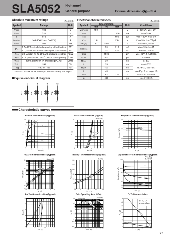
Absolute maximum ratings
Symbol VDSS VGSS ID ID(pulse) EAS* PT Ratings 150 ±20 ±10 ±40 (PW≤1ms, Du≤1%) 160
N-ch...
Description
SLA5052
Absolute maximum ratings
Symbol VDSS VGSS ID ID(pulse) EAS* PT Ratings 150 ±20 ±10 ±40 (PW≤1ms, Du≤1%) 160
N-channel General purpose
(Ta=25°C)
External dimensions A
SLA
(Ta=25°C)
Electrical characteristics
Symbol V(BR)DSS IGSS IDSS VTH Re(yfs) RDS(ON) Ciss Coss td(on) tr td(off) tf VSD trr Specification min typ max 150 ±100 100 1.0 2.0 8 13.5 90 115 105 130 1500 360 30 35 100 40 1.0 1.5 420 Unit V nA µA V S mΩ mΩ pF pF ns ns ns ns V ns
Unit V V A A mJ W W °C/W °C/W Vrms °C °C
Conditions ID=100µA, VGS=0V VGS=±20V VDS=150V, VGS=0V VDS=10V, ID=250µA VDS=10V, ID=5A VGS=10V, ID=5A VGS=4V, ID=5A VDS=10V, f=1.0MHz, VGS=0V ID=5A, VDD 70V, RL=14Ω, VGS=5V, see Fig. 3 on page 16. ISD=10A, VGS=0V ISD=±100mA
θ j–a θ j–c VISO Tch Tstg
5 (Ta=25°C, with all circuits operating, without heatsink) 40 (Tc=25°C,with all circuits operating, with infinite heatsink) 25 (Junction-Air, Ta=25°C, with all circuits operating) 3.13 (Junction-Case, Tc=25°C, with all circuits operating) 1000 (Between fin and lead pin, AC) 150 –40 to +150
* : VDD=25V, L=2.7mH, ID=10A, unclamped, RG=50Ω, see Fig. E on page 15.
sEquivalent circuit diagram
3 6 9 12
1
4
7
10
2
5
8
11
Characteristic curves
ID-VDS Characteristics (Typical)
10
VGS=10V 3.5V
ID-VGS Characteristics (Typical)
(VDS=10V)
10
RDS(ON)-ID Characteristics (Typical)
150
8
3V
8
VGS=4V
(ΩW)
100
ID (A)
ID (A)
6
2.8V
6
TC=–40°C 25°C
10V
4
2.6V
4
125°C
RDS
5
(ON)
50
2
2
0 0
2
4
6
8
10
0 0
1
2
3
4
0 0
...
Similar Datasheet