SML30B40
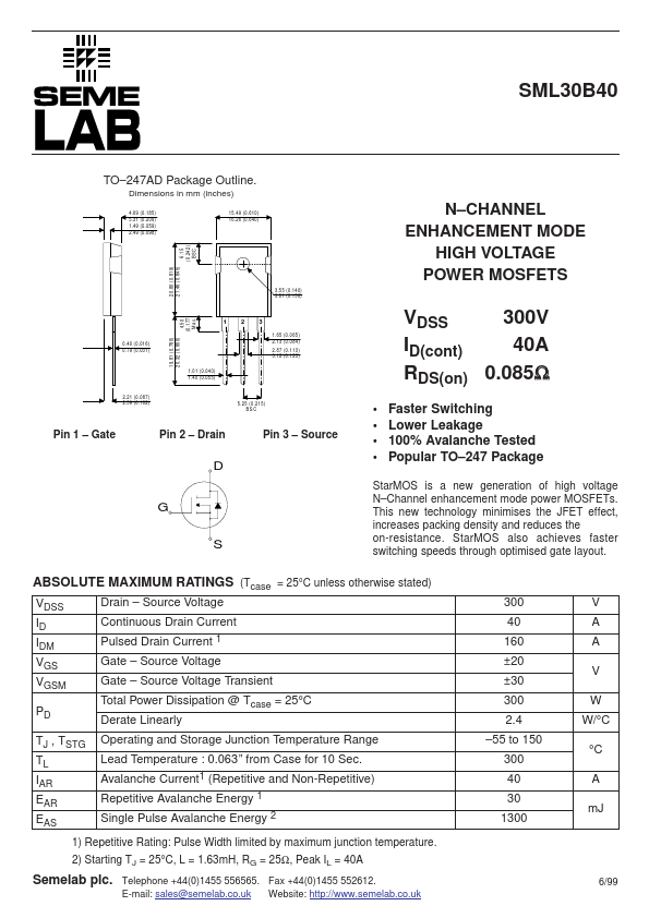
TO–247AD Package Outline.
Dimensions in mm (inches)
4.69 5.31 1.49 2.49 (0.185) (0.209) (0.059) (0.098) 6.15 (...
SML30B40
TO–247AD Package Outline.
Dimensions in mm (inches)
4.69 5.31 1.49 2.49 (0.185) (0.209) (0.059) (0.098) 6.15 (0.242) BSC 15.49 (0.610) 16.26 (0.640)
20.80 (0.819) 21.46 (0.845)
N–CHANNEL ENHANCEMENT MODE HIGH
VOLTAGE POWER
MOSFETS
3.55 (0.140) 3.81 (0.150)
1
2
3
1.65 (0.065) 2.13 (0.084) 2.87 (0.113) 3.12 (0.123)
0.40 (0.016) 0.79 (0.031)
1.01 (0.040) 1.40 (0.055)
VDSS 300V 40A ID(cont) RDS(on) 0.085Ω
Faster Switching Lower Leakage 100% Avalanche Tested Popular TO–247 Package
2.21 (0.087) 2.59 (0.102)
19.81 (0.780) 20.32 (0.800)
4.50 (0.177) M ax.
5.25 (0.215) BSC
Pin 1 – Gate
Pin 2 – Drain
Pin 3 – Source
D
G S
StarMOS is a new generation of high
voltage N–Channel enhancement mode power
MOSFETs. This new technology minimises the JFET effect, increases packing density and reduces the on-resistance. StarMOS also achieves faster switching speeds through optimised gate layout.
ABSOLUTE MAXIMUM RATINGS (Tcase = 25°C unless otherwise stated)
VDSS ID IDM VGS VGSM PD TJ , TSTG TL IAR EAR EAS Drain – Source
Voltage Continuous Drain Current Pulsed Drain Current 1 Gate – Source
Voltage Gate – Source
Voltage Transient Total Power Dissipation @ Tcase = 25°C Derate Linearly Operating and Storage Junction Temperature Range Lead Temperature : 0.063” from Case for 10 Sec. Avalanche Current1 (Repetitive and Non-Repetitive) Repetitive Avalanche Energy 1 Single Pulse Avalanche Energy
2
300 40 160 ±20 ±30 300 2.4 –55 to 150 300 40 30 1300
V A A V W W/°C °C A...