SMP20P10
P-Channel Enhancement-Mode Transistor
Product Summary
V(BR)DSS (V)
–100 TO-220AB
rDS(on) (W)
0.20
ID (A)
–20
...
SMP20P10
P-Channel Enhancement-Mode Transistor
Product Summary
V(BR)DSS (V)
–100 TO-220AB
rDS(on) (W)
0.20
ID (A)
–20
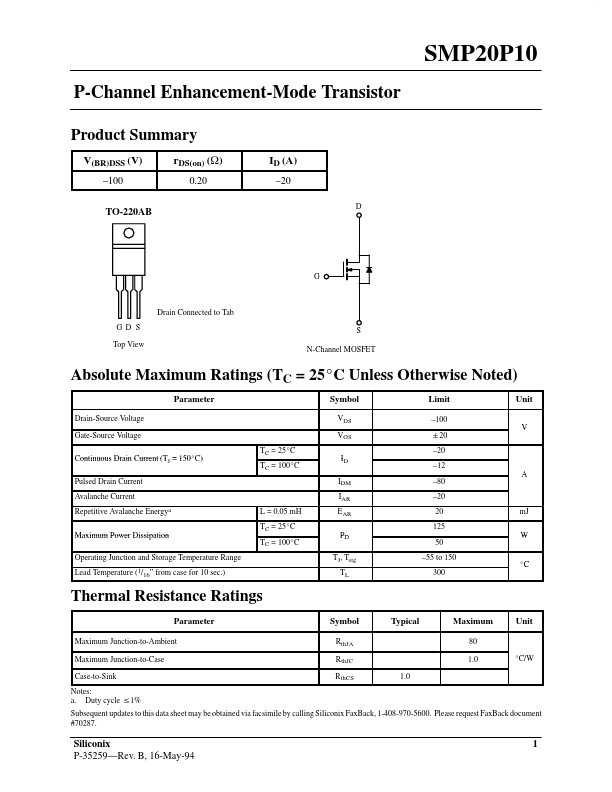
D
G
Drain Connected to Tab G D S Top View S N-Channel
MOSFET
Absolute Maximum Ratings (TC = 25_C Unless Otherwise Noted)
Parameter
Drain-Source
Voltage Gate-Source
Voltage Continuous Drain Current (TJ = 150_C) Pulsed Drain Current Avalanche Current Repetitive Avalanche Energya Maximum Power Dissipation Operating Junction and Storage Temperature Range Lead Temperature (1/16” from case for 10 sec.) L = 0.05 mH TC = 25_C TC = 100_C TC = 25_C TC = 100_C
Symbol
VDS VGS ID IDM IAR EAR PD TJ, Tstg TL
Limit
–100 "20 –20 –12 –80 –20 20 125 50 –55 to 150 300
Unit
V
A
mJ W
_C
Thermal Resistance Ratings
Parameter
Maximum Junction-to-Ambient Maximum Junction-to-Case Case-to-Sink Notes: a. Duty cycle v1% Subsequent updates to this data sheet may be obtained via facsimile by calling Siliconix FaxBack, 1-408-970-5600. Please request FaxBack document #70287.
Symbol
RthJA RthJC RthCS
Typical
Maximum
80 1.0
Unit
_C/W
1.0
Siliconix P-35259—Rev. B, 16-May-94
1
SMP20P10
Specifications (TJ = 25_C Unless Otherwise Noted)
Limit Parameter Static
Drain-Source Breakdown
Voltage Gate Threshold
Voltage Gate-Body Leakage Zero Gate
Voltage Drain Current On-State Drain Currentb Drain Source On-State Drain-Source On State Resistanceb Forward Transconductance b V(BR)DSS VGS(th) IGSS IDSS ID(on) rDS(on) DS( ) gfs VGS = 0 V, ID = –250 mA VDS = VGS, ID = –250 mA VDS = 0 V, VGS...