Quadruple 2-Input Positive-NAND Buffer
SN54ALS03B, SN74ALS03B QUADRUPLE 2ĆINPUT POSITIVEĆNAND BUFFERS
WITH OPENĆCOLLECTOR OUTPUTS
SDAS013B − MARCH 1984 − REVIS...
Description
SN54ALS03B, SN74ALS03B QUADRUPLE 2ĆINPUT POSITIVEĆNAND BUFFERS
WITH OPENĆCOLLECTOR OUTPUTS
SDAS013B − MARCH 1984 − REVISED DECEMBER 1994
Package Options Include Plastic
Small-Outline (D) Packages, Ceramic Chip Carriers (FK), and Standard Plastic (N) and Ceramic (J) 300-mil DIPs
description
These devices contain four independent 2-input positive-NAND buffers. They perform the Boolean functions Y = A B or Y = A + B in positive logic. The open-collector outputs require pullup resistors to perform correctly. These outputs may be connected to other open-collector outputs to implement active-low wired-OR or active-high wired-AND functions. Open-collector devices are often used to generate high VOH levels.
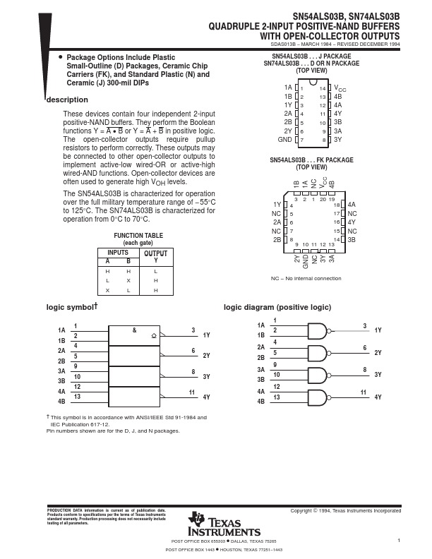
SN54ALS03B . . . J PACKAGE SN74ALS03B . . . D OR N PACKAGE
(TOP VIEW)
1A 1 1B 2 1Y 3 2A 4 2B 5 2Y 6 GND 7
14 VCC 13 4B 12 4A 11 4Y 10 3B 9 3A 8 3Y
SN54ALS03B . . . FK PACKAGE (TOP VIEW)
4B
VCC
NC
1A
1B
The SN54ALS03B is characterized for operation over the full military temperature range of − 55°C to 125°C. The SN74ALS03B is characterized for operation from 0°C to 70°C.
FUNCTION TABLE (each gate)
INPUTS
A
B
OUTPUT Y
2Y
NC
3 2 1 20 19
1Y 4
18 4A
NC 5
17 NC
2A 6
16 4Y
NC 7
15 NC
2B 8
14 3B
9 10 11 12 13
3Y
3A
GND
H
H
L
L
X
H
NC − No internal connection
X
L
H
logic symbol†
1
1A
&
2
1B
4
2A
5
2B
9
3A
10
3B
12
4A
13
4B
3 1Y
6 2Y
8 3Y
11 4Y
logic diagram (positive logic)
1 1A
2 1B
4 2A
5 2B
9 3A
10 3B
12 4A
13 4B
3 1Y
6...
Similar Datasheet