8-Bit Universal Shift/Storage Registers
SN54ALS323, SN74ALS323 8ĆBIT UNIVERSAL SHIFT/STORAGE REGISTERS WITH SYNCHRONOUS CLEAR AND 3ĆSTATE OUTPUTS
SDAS267A − DEC...
Description
SN54ALS323, SN74ALS323 8ĆBIT UNIVERSAL SHIFT/STORAGE REGISTERS WITH SYNCHRONOUS CLEAR AND 3ĆSTATE OUTPUTS
SDAS267A − DECEMBER 1982 − REVISED DECEMBER 1994
Multiplexed I/O Ports Provide Improved Bit
Density
Four Modes of Operation:
− Hold (Store) − Shift Right − Shift Left − Load Data
Operate With Outputs Enabled or at High
Impedance
3-State Outputs Drive Bus Lines Directly Can Be Cascaded for n-Bit Word Lengths Synchronous Clear Applications:
− Stacked or Push-Down Registers − Buffer Storage − Accumulator Registers
Package Options Include Plastic
Small-Outline (DW) Packages, Ceramic Chip Carriers (FK), and Standard Plastic (N) and Ceramic (J) 300-mil DIPs
description
These 8-bit universal shift /storage registers feature multiplexed input/output (I/O) ports to achieve full 8-bit data handling in a 20-pin package. Two function-select (S0, S1) inputs and two output-enable (OE1, OE2) inputs can be used to choose the modes of operation listed in the function table.
CLR GND
SR CLK B/QB
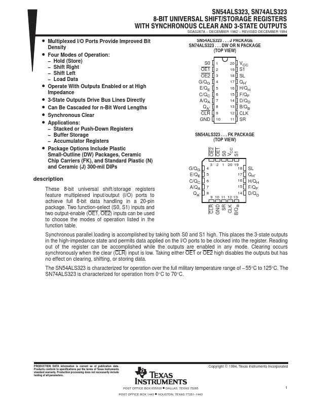
SN54ALS323 . . . J PACKAGE SN74ALS323 . . . DW OR N PACKAGE
(TOP VIEW)
S0
OE1
OE2
G/QG E/QE C/QC A/QA
QA′ CLR
GND
1 2 3 4 5 6 7 8 9 10
20 VCC 19 S1
18 SL
17 QH′ 16 H/QH 15 F/QF 14 D/QD 13 B/QB 12 CLK
11 SR
SN54ALS323 . . . FK PACKAGE (TOP VIEW)
OE2 OE1 S0 VCC S1
G/QG E/QE C/QC A/QA
QA′
3 2 1 20 19 4 18
5 17
6 16
7 15
8 14 9 10 11 12 13
SL
QH′ H/QH F/QF D/QD
Synchronous parallel loading is accomplished by taking both S0 and S1 high. This places the 3-state outputs in the h...
Similar Datasheet