OCTAL BUFFERS AND LINE DRIVER
D 3-State Outputs Drive Bus Lines or Buffer
Memory Address Registers
D pnp Inputs Reduce dc Loading D Data Flowthrough P...
Description
D 3-State Outputs Drive Bus Lines or Buffer
Memory Address Registers
D pnp Inputs Reduce dc Loading D Data Flowthrough Pinout (All Inputs on
Opposite Side From Outputs)
description
These octal buffers and line drivers are designed to have the performance of the popular SN54ALS240A/ SN74ALS240A series and, at the same time, offer a pinout with inputs and outputs on opposite sides of the package. This arrangement greatly facilitates printed circuit board layout.
The 3-state control gate is a 2-input NOR gate such that, if either output-enable (OE1 or OE2) input is high, all eight outputs are in the high-impedance state.
The SN74ALS540 provides inverted data. The ’ALS541 provide true data at the outputs.
The -1 versions of SN74ALS540 and SN74ALS541 are identical to the standard versions, except that the recommended maximum IOL is increased to 48 mA. There is no -1 version of the SN54ALS541.
SN54ALS541, SN74ALS540, SN74ALS541
OCTAL BUFFERS AND LINE DRIVERS WITH 3-STATE OUTPUTS
SDAS025D – APRIL 1982 – REVISED MARCH 2002
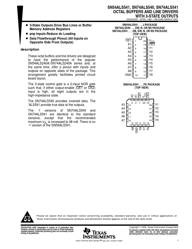
SN54ALS541 . . . J PACKAGE SN74ALS540 . . . DW, N, OR NS PACKAGE SN74ALS541 . . . DB, DW, N, OR NS PACKAGE
(TOP VIEW)
OE1 1 A1 2 A2 3 A3 4 A4 5 A5 6 A6 7 A7 8 A8 9
GND 10
20 VCC 19 OE2 18 Y1 17 Y2 16 Y3 15 Y4 14 Y5 13 Y6 12 Y7 11 Y8
SN54ALS541 . . . FK PACKAGE (TOP VIEW)
A2 A1 OE1 VCC OE2
A3
3 2 1 20 19
4
18
Y1
A4 5
17 Y2
A5 6
16 Y3
A6 7
15 Y4
A7 8
14 Y5
9 10 11 12 13
A8 GND
Y8 Y7 Y6
Please be aware that an important notice concerning availabi...
Similar Datasheet