Quadruple 2-Input Positive-OR Buffers/Drivers
SN54AS1032A, SN74AS1032A QUADRUPLE 2ĆINPUT POSITIVEĆOR BUFFERS/DRIVERS
• Driver Version of ′AS32 • High Capacitive-Driv...
Description
SN54AS1032A, SN74AS1032A QUADRUPLE 2ĆINPUT POSITIVEĆOR BUFFERS/DRIVERS
Driver Version of ′AS32 High Capacitive-Drive Capability Package Options Include Plastic
Small-Outline (D) Packages, Ceramic Chip
Carriers (FK), and Standard Plastic (N) and
Ceramic (J) 300-mil DIPs
description
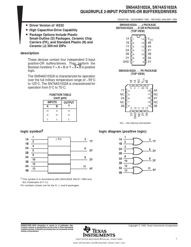
These devices contain four independent 2-input positive-OR buffers/drivers. They perform the Boolean functions Y = A + B or Y = A B in positive logic.
The SN54AS1032A is characterized for operation over the full military temperature range of − 55°C to 125°C. The SN74AS1032A is characterized for operation from 0°C to 70°C.
FUNCTION TABLE (each gate)
INPUTS
A
B
OUTPUT Y
H
X
H
X
H
H
L
L
L
SDAS072B − DECEMBER 1982 − REVISED JANUARY 1995
SN54AS1032A . . . J PACKAGE SN74AS1032A . . . D OR N PACKAGE
(TOP VIEW)
1A 1 1B 2 1Y 3 2A 4 2B 5 2Y 6 GND 7
14 VCC 13 4B 12 4A 11 4Y 10 3B 9 3A 8 3Y
SN54AS1032A . . . FK PACKAGE (TOP VIEW)
4B
VCC
NC
1A
1B
3 2 1 20 19
1Y 4
18 4A
NC 5
17 NC
2A 6
16 4Y
NC 7
15 NC
2B 8
14 3B
9 10 11 12 13
3A
3Y
NC
GND
2Y
NC − No internal connection
logic symbol†
1
1A
≥1
2
1B
4
2A
5
2B
9
3A
10
3B
12
4A
13
4B
3 1Y
6 2Y
8 3Y
11 4Y
† This symbol is in accordance with ANSI/IEEE Std 91-1984 and IEC Publication 617-12.
Pin numbers shown are for the D, J, and N packages.
logic diagram (positive logic)
1 1A
2 1B
4 2A
5 2B
9 3A
10 3B
12 4A
13 4B
3 1Y
6 2Y
8 3Y 11 4Y
PRODUCTION DATA information is current as of publication date....
Similar Datasheet