• BiCMOS Design Substantially Reduces ICCZ • Functionally Equivalent to ′ALS29863 and
AMD Am29863A
• Power-Up High-Imped...
Bi
CMOS Design Substantially Reduces ICCZ Functionally Equivalent to ′ALS29863 and
AMD Am29863A
Power-Up High-Impedance State ESD Protection Exceeds 2000 V Per
MIL-STD-883C, Method 3015
Package Options Include Plastic
Small-Outline Packages (DW), Ceramic Chip Carriers (FK) and Flatpacks (W), and Standard Plastic and Ceramic 300-mil DIPs (JT, NT)
description
These 9-bit transceivers are designed for asynchronous communication between data buses. The control-function implementation allows for maximum flexibility in timing.
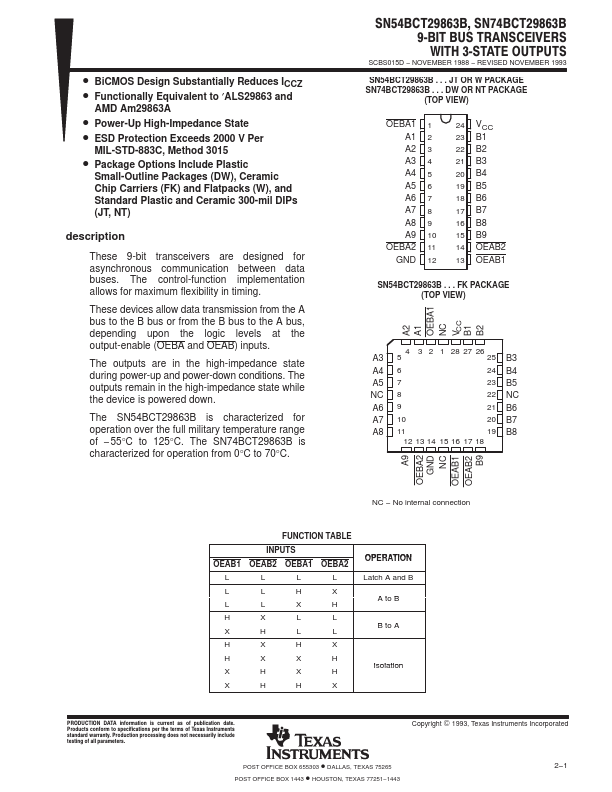
These devices allow data transmission from the A bus to the B bus or from the B bus to the A bus, depending upon the logic levels at the output-enable (OEBA and OEAB) inputs.
The outputs are in the high-impedance state during power-up and power-down conditions. The outputs remain in the high-impedance state while the device is powered down.
The SN54BCT29863B is characterized for operation over the full military temperature range of − 55°C to 125°C. The SN74BCT29863B is characterized for operation from 0°C to 70°C.
SN54BCT29863B, SN74BCT29863B 9ĆBIT BUS TRANSCEIVERS WITH 3ĆSTATE OUTPUTS
SCBS015D − NOVEMBER 1988 − REVISED NOVEMBER 1993
SN54BCT29863B . . . JT OR W PACKAGE SN74BCT29863B . . . DW OR NT PACKAGE
(TOP VIEW)
OEBA1 1 A1 2 A2 3 A3 4 A4 5 A5 6 A6 7 A7 8 A8 9 A9 10
OEBA2 11 GND 12
24 VCC 23 B1 22 B2 21 B3 20 B4 19 B5 18 B6 17 B7 16 B8 15 B9 14 OEAB2 13 OEAB1
SN54BCT29863B . . . FK PACKAGE (TOP VIEW)
A2 A1 OEBA1 NC VCC B1 B2
4 3 2 1 28 27 26...