10-BIT FET BUS SWITCHES
D 5-Ω Switch Connection Between Two Ports D TTL-Compatible Input Levels
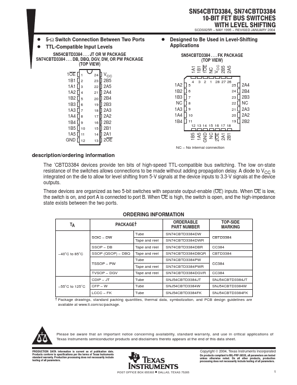
SN54CBTD3384 . . . JT OR W PACKAGE SN74CBTD3384 ...
Description
D 5-Ω Switch Connection Between Two Ports D TTL-Compatible Input Levels
SN54CBTD3384 . . . JT OR W PACKAGE SN74CBTD3384 . . . DB, DBQ, DGV, DW, OR PW PACKAGE
(TOP VIEW)
SN54CBTD3384, SN74CBTD3384 10ĆBIT FET BUS SWITCHES WITH LEVEL SHIFTING
SCDS025R − MAY 1995 − REVISED JANUARY 2004
D Designed to Be Used in Level-Shifting
Applications
SN54CBTD3384 . . . FK PACKAGE (TOP VIEW)
1A1 1B1 1OE NC VCC 2B5 2A5
1OE 1 1B1 2 1A1 3 1A2 4 1B2 5 1B3 6 1A3 7 1A4 8 1B4 9 1B5 10 1A5 11 GND 12
24 VCC 23 2B5 22 2A5 21 2A4 20 2B4 19 2B3 18 2A3 17 2A2 16 2B2 15 2B1 14 2A1 13 2OE
description/ordering information
4 3 2 1 28 27 26
1A2 5
25 2A4
1B2 6
24 2B4
1B3 7
23 2B3
NC 8
22 NC
1A3 9
21 2A3
1A4 10
20 2A2
1B4 11
19 2B2
12 13 14 15 16 17 18
1B5 1A5 GND NC 2OE 2A1 2B1
NC − No internal connection
The ’CBTD3384 devices provide ten bits of high-speed TTL-compatible bus switching. The low on-state resistance of the switches allows connections to be made without adding propagation delay. A diode to VCC is integrated on the die to allow for level shifting from 5-V signals at the device inputs to 3.3-V signals at the device outputs.
These devices are organized as two 5-bit switches with separate output-enable (OE) inputs. When OE is low, the switch is on, and port A is connected to port B. When OE is high, the switch is open, and the high-impedance state exists between the two ports.
ORDERING INFORMATION
TA
PACKAGE†
ORDERABLE PART NUMBER
TOP-SIDE MARKING
SOIC − DW
Tube Tape and ...
Similar Datasheet