D Operating Voltage Range of 4.5 V to 5.5 V D Low Power Consumption, 80-µA Max ICC D Typical tpd = 12 ns D ±6-mA Output ...
D Operating
Voltage Range of 4.5 V to 5.5 V D Low Power Consumption, 80-µA Max ICC D Typical tpd = 12 ns D ±6-mA Output Drive at 5 V D Low Input Current of 1 µA Max D Inputs Are TTL-
Voltage Compatible D High-Current 3-State Outputs Interface
Directly With System Bus or Can Drive Up To 15 LSTTL Loads
D Data Flow-Through Pinout (All Inputs on
Opposite Side From Outputs)
description/ordering information
SN54HCT540, SN74HCT540 OCTAL BUFFERS AND LINE DRIVERS
WITH 3-STATE OUTPUTS
SCLS008C – MARCH 1984 – REVISED MARCH 2003
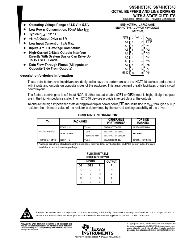
SN54HCT540 . . . J PACKAGE SN74HCT540 . . . DW OR N PACKAGE
(TOP VIEW)
OE1 1 A1 2 A2 3 A3 4 A4 5 A5 6 A6 7 A7 8 A8 9
GND 10
20 VCC 19 OE2 18 Y1 17 Y2 16 Y3 15 Y4 14 Y5 13 Y6 12 Y7 11 Y8
These octal buffers and line drivers are designed to have the performance of the ’HCT240 devices and a pinout with inputs and outputs on opposite sides of the package. This arrangement greatly facilitates printed circuit board layout.
The 3-state control gate is a 2-input NOR. If either output-enable (OE1 or OE2) input is high, all eight outputs are in the high-impedance state. The ’HCT540 devices provide inverted data at the outputs.
To ensure the high-impedance state during power up or power down, OE should be tied to VCC through a pullup resistor; the minimum value of the resistor is determined by the current-sinking capability of the driver.
ORDERING INFORMATION
TA
PACKAGE†
ORDERABLE PART NUMBER
TOP-SIDE MARKING
PDIP – N
Tube
SN74HCT540N
SN74HCT540N
–40°C to 85°C
...