D Operating Voltage Range of 4.5 V to 5.5 V D Low Power Consumption, 80-µA Max ICC D Typical tpd = 12 ns D ±6-mA Output ...
D Operating
Voltage Range of 4.5 V to 5.5 V D Low Power Consumption, 80-µA Max ICC D Typical tpd = 12 ns D ±6-mA Output Drive at 5 V D Low Input Current of 1 µA Max D Inputs Are TTL-
Voltage Compatible
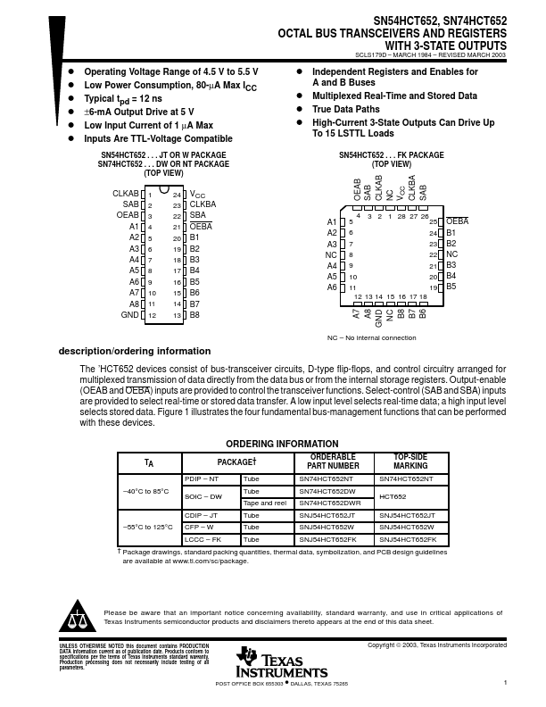
SN54HCT652 . . . JT OR W PACKAGE SN74HCT652 . . . DW OR NT PACKAGE
(TOP VIEW)
CLKAB 1 SAB 2
OEAB 3 A1 4 A2 5 A3 6 A4 7 A5 8 A6 9 A7 10 A8 11
GND 12
24 VCC 23 CLKBA 22 SBA 21 OEBA 20 B1 19 B2 18 B3 17 B4 16 B5 15 B6 14 B7 13 B8
SN54HCT652, SN74HCT652 OCTAL BUS TRANSCEIVERS AND REGISTERS
WITH 3-STATE OUTPUTS
SCLS179D – MARCH 1984 – REVISED MARCH 2003
D Independent Registers and Enables for
A and B Buses
D Multiplexed Real-Time and Stored Data D True Data Paths D High-Current 3-State Outputs Can Drive Up
To 15 LSTTL Loads
SN54HCT652 . . . FK PACKAGE (TOP VIEW)
OEAB SAB CLKAB NC VCC CLKBA SAB
4 3 2 1 28 27 26
A1 5
25 OEBA
A2 6
24 B1
A3 7
23 B2
NC 8
22 NC
A4 9
21 B3
A5 10
20 B4
A6 11
19 B5
12 13 14 15 16 17 18
A7 A8 GND NC B8 B7 B6
description/ordering information
NC – No internal connection
The ’HCT652 devices consist of bus-transceiver circuits, D-type flip-flops, and control circuitry arranged for multiplexed transmission of data directly from the data bus or from the internal storage registers. Output-enable (OEAB and OEBA) inputs are provided to control the transceiver functions. Select-control (SAB and SBA) inputs are provided to select real-time or stored data transfer. A low input level selects real-time data; a high input level selects stored data. Fi...