SN54/74LS73A DUAL JK NEGATIVE EDGE-TRIGGERED FLIP-FLOP
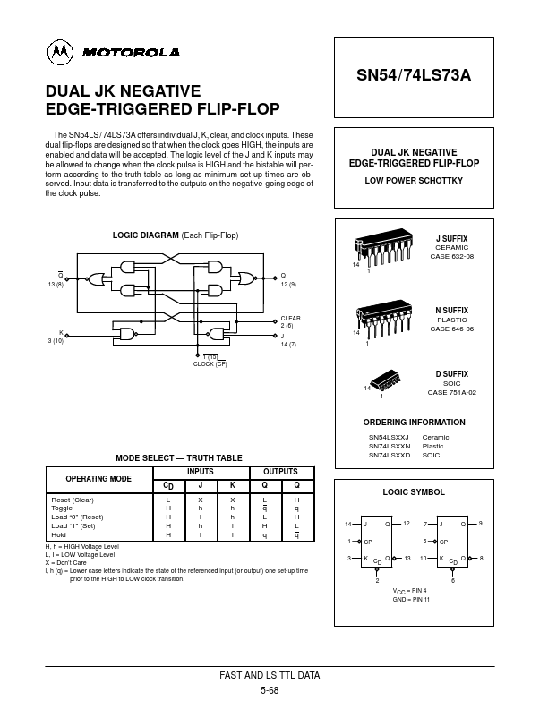
The SN54LS / 74LS73A offers individual J, K, clear, and clock inp...
SN54/74LS73A DUAL JK NEGATIVE EDGE-TRIGGERED FLIP-FLOP
The SN54LS / 74LS73A offers individual J, K, clear, and clock inputs. These dual flip-flops are designed so that when the clock goes HIGH, the inputs are enabled and data will be accepted. The logic level of the J and K inputs may be allowed to change when the clock pulse is HIGH and the bistable will perform according to the truth table as long as minimum set-up times are observed. Input data is transferred to the outputs on the negative-going edge of the clock pulse.
DUAL JK NEGATIVE EDGE-TRIGGERED FLIP-FLOP
LOW POWER SCHOTTKY
LOGIC DIAGRAM (Each Flip-Flop)
J SUFFIX CERAMIC CASE 632-08
14
Q 13 (8)
Q 12 (9)
1
CLEAR 2 (6) K 3 (10) 1 (15) CLOCK (CP) J 14 (7)
14 1
N SUFFIX PLASTIC CASE 646-06
14 1
D SUFFIX SOIC CASE 751A-02
ORDERING INFORMATION
SN54LSXXJ SN74LSXXN SN74LSXXD OUTPUTS K X h h l l Q L q L H q Q H q H L q Ceramic Plastic SOIC
MODE SELECT — TRUTH TABLE
INPUTS OPERATING MODE CD Reset (Clear) Toggle Load “0” (Reset) Load “1” (Set) Hold L H H H H J X h l h l
LOGIC SYMBOL
14 1 3
J CP
Q
12
7 5
J CP
Q
9
H, h = HIGH
Voltage Level L, I = LOW
Voltage Level X = Don’t Care l, h (q) = Lower case letters indicate the state of the referenced input (or output) one set-up time l, h (q) = prior to the HIGH to LOW clock transition.
K C Q D 2
13
10
K C Q D 6
8
VCC = PIN 4 GND = PIN 11
FAST AND LS TTL DATA 5-68
SN54/74LS73A
GUARANTEED OPERATING RANGES
Symbol VCC TA IOH IOL Supply
Voltage Operating Ambie...