SN54LV4066A, SN74LV4066A QUADRUPLE BILATERAL ANALOG SWITCHES
D 2-V to 5.5-V VCC Operation D Support Mixed-Mode Voltage ...
SN54LV4066A, SN74LV4066A QUADRUPLE BILATERAL ANALOG SWITCHES
D 2-V to 5.5-V VCC Operation D Support Mixed-Mode
Voltage Operation on
All Ports
D High On-Off Output-
Voltage Ratio D Low Crosstalk Between Switches D Individual Switch Controls D Extremely Low Input Current D ESD Protection Exceeds JESD 22
− 2000-V Human-Body Model (A114-A) − 200-V Machine Model (A115-A) − 1000-V Charged-Device Model (C101)
description/ordering information
This quadruple silicon-gate
CMOS analog switch is designed for 2-V to 5.5-V VCC operation.
These switches are designed to handle both analog and digital signals. Each switch permits signals with amplitudes up to 5.5 V (peak) to be transmitted in either direction.
Each switch section has its own enable-input control (C). A high-level
voltage applied to C turns on the associated switch section.
Applications include signal gating, chopping, modulation or demodulation (modem), and signal multiplexing for analog-to-digital and digital-to-analog conversion systems.
SCLS427I − APRIL 1999 − REVISED APRIL 2005
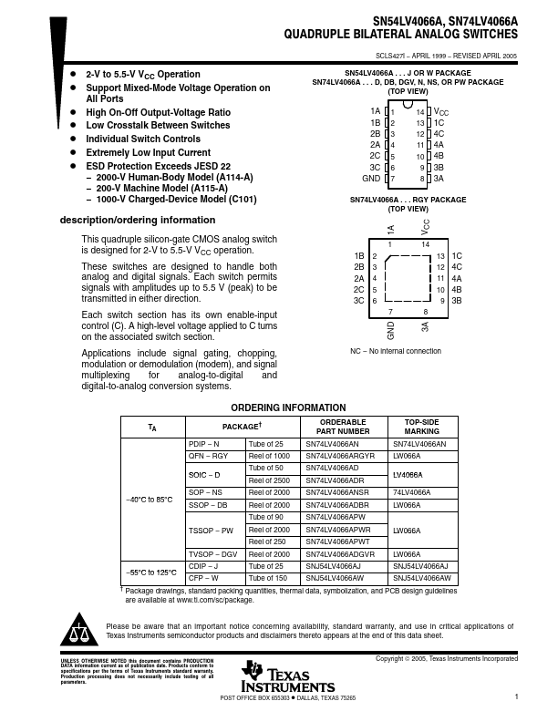
SN54LV4066A . . . J OR W PACKAGE SN74LV4066A . . . D, DB, DGV, N, NS, OR PW PACKAGE
(TOP VIEW)
1A 1 1B 2 2B 3 2A 4 2C 5 3C 6 GND 7
14 VCC 13 1C 12 4C 11 4A 10 4B 9 3B 8 3A
SN74LV4066A . . . RGY PACKAGE (TOP VIEW)
VCC
1A
1 1B 2 2B 3 2A 4 2C 5 3C 6
7
14 13 1C 12 4C 11 4A 10 4B 9 3B
8
3A
GND
NC − No internal connection
ORDERING INFORMATION
TA
PACKAGE†
ORDERABLE PART NUMBER
TOP-SIDE MARKING
−40°C to 85°C
PDIP − N QFN − RGY
SOIC − D
SO...