SN54LVTH374, SN74LVTH374 3.3ĆV ABT OCTAL EDGEĆTRIGGERED DĆTYPE FLIPĆFLOPS
WITH 3ĆSTATE OUTPUTS
SCBS683H − MARCH 1997 − R...
SN54LVTH374, SN74LVTH374 3.3ĆV ABT OCTAL EDGEĆTRIGGERED DĆTYPE FLIPĆFLOPS
WITH 3ĆSTATE OUTPUTS
SCBS683H − MARCH 1997 − REVISED OCTOBER 2003
D Support Mixed-Mode Signal Operation
(5-V Input and Output
Voltages With 3.3-V VCC)
D Typical VOLP (Output Ground Bounce)
<0.8 V at VCC = 3.3 V, TA = 25°C
D Support Unregulated Battery Operation
Down to 2.7 V
D Ioff and Power-Up 3-State Support Hot
Insertion
D Bus Hold on Data Inputs Eliminates the
Need for External Pullup/Pulldown Resistors
D Latch-Up Performance Exceeds 500 mA Per
JESD 17
D ESD Protection Exceeds JESD 22
− 2000-V Human-Body Model (A114-A) − 200-V Machine Model (A115-A)
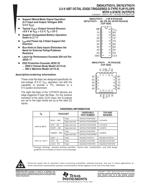
SN54LVTH374 . . . J OR W PACKAGE SN74LVTH374 . . . DB, DW, NS, OR PW PACKAGE
(TOP VIEW)
OE 1 1Q 2 1D 3 2D 4 2Q 5 3Q 6 3D 7 4D 8 4Q 9 GND 10
20 VCC 19 8Q 18 8D 17 7D 16 7Q 15 6Q 14 6D 13 5D 12 5Q 11 CLK
SN54LVTH374 . . . FK PACKAGE (TOP VIEW)
8Q
VCC
OE
1Q
1D
description/ordering information
These octal flip-flops are designed specifically for low-
voltage (3.3-V) VCC operation, but with the capability to provide a TTL interface to a 5-V system environment.
The eight flip-flops of the ’LVTH374 devices are edge-triggered D-type flip-flops. On the positive transition of the clock (CLK) input, the Q outputs are set to the logic levels set up at the data (D) inputs.
4Q
GND
CLK
2D
3 2 1 20 19
4
18
8D
2Q 5
17 7D
3Q 6
16 7Q
3D 7
15 6Q
4D 8
14 6D
9 10 11 12 13
5Q
5D
ORDERING INFORMATION
TA
PACKAGE†
ORDERABLE PART NUMBER
TOP-SIDE M...