SN55LBC173 QUADRUPLE LOW-POWER DIFFERENTIAL RECEIVER
SGLS081A – MARCH 1995 – REVISED JUNE 2000
D Meets EIA Standards R...
SN55LBC173 QUADRUPLE LOW-POWER DIFFERENTIAL RECEIVER
SGLS081A – MARCH 1995 – REVISED JUNE 2000
D Meets EIA Standards RS-422-A, RS-423-A,
RS-485, and CCITT V.11
D Designed to Operate With Pulse Durations
as Short as 20 ns
D Designed for Multipoint Bus Transmission
on Long Bus Lines in Noisy Environments
D Input Sensitivity . . . ± 200 mV D Low-Power Consumption . . . 20 mA Max D Open-Circuit Fail-Safe Design D Pin Compatible With SN75173 and
AM26LS32
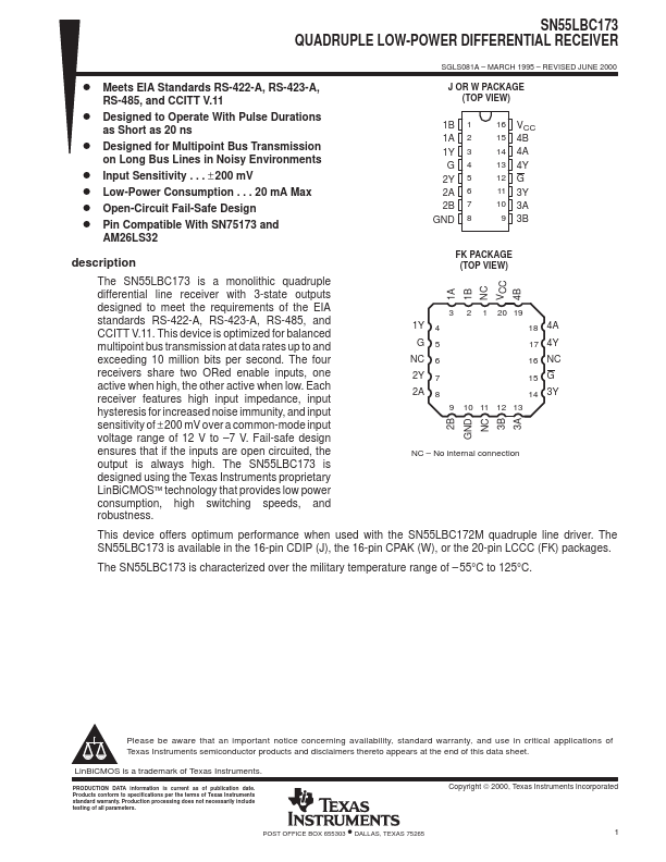
J OR W PACKAGE (TOP VIEW)
1B 1 1A 2 1Y 3 G4 2Y 5 2A 6 2B 7 GND 8
16 VCC 15 4B 14 4A 13 4Y 12 G 11 3Y 10 3A 9 3B
description
The SN55LBC173 is a monolithic quadruple differential line receiver with 3-state outputs designed to meet the requirements of the EIA standards RS-422-A, RS-423-A, RS-485, and CCITT V.11. This device is optimized for balanced multipoint bus transmission at data rates up to and exceeding 10 million bits per second. The four receivers share two ORed enable inputs, one active when high, the other active when low. Each receiver features high input impedance, input hysteresis for increased noise immunity, and input sensitivity of ± 200 mV over a common-mode input
voltage range of 12 V to –7 V. Fail-safe design ensures that if the inputs are open circuited, the output is always high. The SN55LBC173 is designed using the Texas Instruments proprietary LinBi
CMOS™ technology that provides low power consumption, high switching speeds, and robustness.
FK PACKAGE (TOP VIEW)
1A 1B NC VCC 4B
3 2 1 20 19
1Y 4
18 4...