ą
• Each Device Drives 32 Lines • 60-V Output Voltage Swing Capability • 25-mA Output Source Current Capability • High-S...
ą
Each Device Drives 32 Lines 60-V Output
Voltage Swing Capability 25-mA Output Source Current Capability High-Speed Serially Shifted Data Input Latches on All Driver Outputs
description
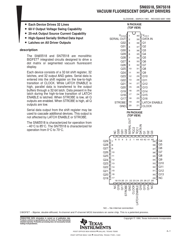
The SN65518 and SN75518 are monolithic BIDFET† integrated circuits designed to drive a dot matrix or segmented vacuum fluorescent display.
Each device consists of a 32-bit shift register, 32 latches, and 32 output AND gates. Serial data is entered into the shift register on the low-to-high transition of CLOCK. While LATCH ENABLE is high, parallel data is transferred to the output buffers through a 32-bit latch. Data present in the latch during the high-to-low transition of LATCH ENABLE is latched. When STROBE is low, all Q outputs are enabled. When STROBE is high, all Q outputs are low.
Serial data output from the shift register may be used to cascade additional devices. This output is not affected by LATCH ENABLE or STROBE.
The SN65518 is characterized for operation from −40°C to 85°C. The SN75518 is characterized for operation from 0°C to 70°C.
SN65518, SN75518 VACUUM FLUORESCENT DISPLAY DRIVERS
ą
SLDS004B − MARCH 1983 − REVISED MAY 1990
N PACKAGE (TOP VIEW)
VCC2 SERIAL OUT
Q32 Q31 Q30 Q29 Q28 Q27 Q26 Q25 Q24 Q23 Q22 Q21 Q20 Q19 Q18 Q17 STROBE GND
1 2 3 4 5 6 7 8 9 10 11 12 13 14 15 16 17 18 19 20
40 VCC1 39 DATA IN 38 Q1 37 Q2
36 Q3
35 Q4
34 Q5
33 Q6
32 Q7
31 Q8 30 Q9 29 Q10 28 Q11 27 Q12 26 Q13 25 Q14 24 Q15 23 Q16 22 LATCH ENABLE 21 CLOCK
FN PACKAGE (TOP VIEW)
NC Q30 Q31 ...