SN65LBC180A SN75LBC180A
www.ti.com.........................................................................................
SN65LBC180A SN75LBC180A
www.ti.com............................................................................................................................................................... SLLS378D – MAY 2000 – REVISED APRIL 2009
LOW-POWER DIFFERENTIAL LINE DRIVER AND RECEIVER PAIRS
FEATURES
1
2 High-Speed Low-Power LinBI
CMOS™ Circuitry Designed for Signaling Rates(1) of up to 30 Mbps
Bus-Pin ESD Protection 15 kV HBM Low Disabled Supply-Current Requirements:
700 µA Maximum Designed for High-Speed Multipoint Data
Transmission Over Long Cables
Common-Mode
Voltage Range of –7 V to 12 V Low Supply Current: 15 mA Max Compatible With ANSI Standard TIA/EIA-485-A
and ISO 8482:1987(E)
Positive and Negative Output Current Limiting Driver Thermal Shutdown Protection
(1) Signaling rate by TIA/EIA-485-A definition restrict transition times to 30% of the bit duration, and much higher signaling rates may be achieved without this requirement as displayed in the TYPICAL CHARACTERISTICS of this device.
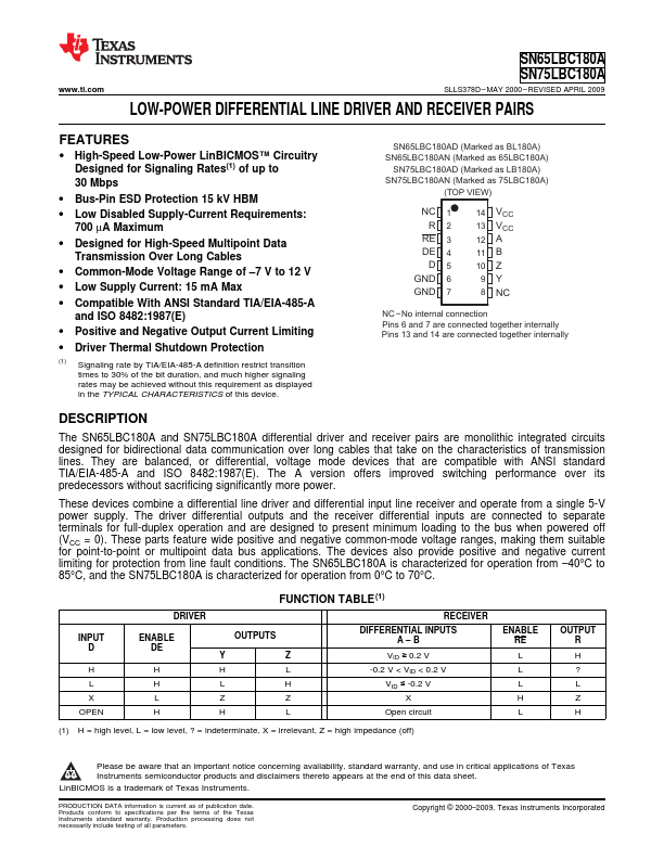
SN65LBC180AD (Marked as BL180A) SN65LBC180AN (Marked as 65LBC180A)
SN75LBC180AD (Marked as LB180A) SN75LBC180AN (Marked as 75LBC180A)
(TOP VIEW)
NC 1 R2
RE 3 DE 4
D5 GND 6 GND 7
14 VCC 13 VCC 12 A 11 B 10 Z 9Y 8 NC
NC −No internal connection Pins 6 and 7 are connected together internally Pins 13 and 14 are connected together internally
DESCRIPTION
The SN65LBC180A and SN75LBC180A differential driver and receiver pairs are monolithic integrated circuits designed for bid...