D Members of the Texas Instruments
Widebus™ Family
D State-of-the-Art EPIC-ΙΙB™ BiCMOS Design
Significantly Reduces Powe...
D Members of the Texas Instruments
Widebus™ Family
D State-of-the-Art EPIC-ΙΙB™ Bi
CMOS Design
Significantly Reduces Power Dissipation
D Latch-Up Performance Exceeds 500 mA Per
JEDEC Standard JESD-17
D Typical VOLP (Output Ground Bounce) < 1 V
at VCC = 5 V, TA = 25°C
D Distributed VCC and GND Pin Configuration
Minimizes High-Speed Switching Noise
D Flow-Through Architecture Optimizes PCB
Layout
D High-Drive Outputs (–32-mA IOH, 64-mA IOL) D Package Options Include Plastic 300-mil
Shrink Small-Outline (DL) and Thin Shrink Small-Outline (DGG) Packages and 380-mil Fine-Pitch Ceramic Flat (WD) Package Using 25-mil Center-to-Center Spacings
description
The ’ABT16470 are 16-bit registered transceivers that contain two sets of D-type flip-flops for temporary storage of data flowing in either direction. The ’ABT16470 can be used as two 8-bit transceivers or one 16-bit transceiver. Separate clock (CLKAB or CLKBA) and output-enable (OEAB or OEBA) inputs are provided for each register to permit independent control in either direction of data flow.
To avoid false clocking of the flip-flops, clock enable (CLKEN) should not be switched from high to low while CLK is high.
SN54ABT16470, SN74ABT16470 16-BIT REGISTERED TRANSCEIVERS
WITH 3-STATE OUTPUTS
SCBS085E – FEBRUARY 1991 – REVISED MAY 1997
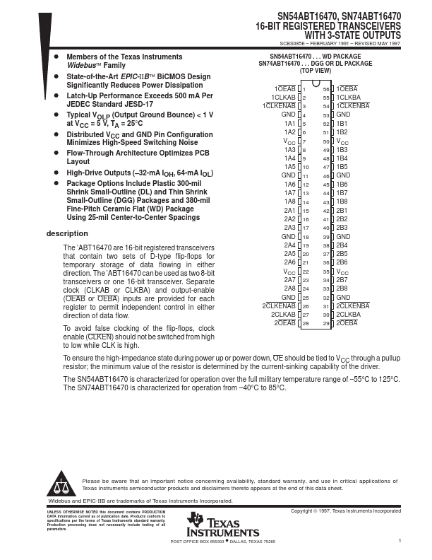
SN54ABT16470 . . . WD PACKAGE SN74ABT16470 . . . DGG OR DL PACKAGE
(TOP VIEW)
1OEAB 1 1CLKAB 2 1CLKENAB 3
GND 4 1A1 5 1A2 6 VCC 7 1A3 8 1A4 9 1A5 10 GND 11 1A6 12 1A7 13 1A8 14 2A1 15 2A2 16 2A3 17 GN...