D Members of the Texas Instruments
Widebus™ Family
D State-of-the-Art EPIC-ΙΙB™ BiCMOS Design
Significantly Reduces Powe...
D Members of the Texas Instruments
Widebus™ Family
D State-of-the-Art EPIC-ΙΙB™ Bi
CMOS Design
Significantly Reduces Power Dissipation
D Latch-Up Performance Exceeds 500 mA Per
JEDEC Standard JESD-17
D Typical VOLP (Output Ground Bounce)
< 1 V at VCC = 5 V, TA = 25°C
D Distributed VCC and GND Pin Configuration
Minimizes High-Speed Switching Noise
D Flow-Through Architecture Optimizes PCB
Layout
D High-Drive Outputs (–32-mA IOH, 64-mA IOL) D Package Options Include Plastic 300-mil
Shrink Small-Outline (DL), Thin Shrink Small-Outline (DGG), and Thin Very Small-Outline (DGV) Packages, and 380-mil Fine-Pitch Ceramic Flat (WD) Package Using 25-mil Center-to-Center Spacings
description
The SN54ABT16540 and SN74ABT16540A are inverting 16-bit buffers/drivers composed of two 8-bit sections with separate output-enable gates. These buffers and bus drivers provide a high-performance bus interface for wide data paths.
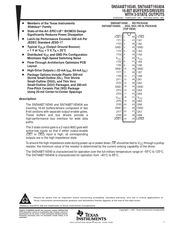
SN54ABT16540, SN74ABT16540A 16-BIT BUFFERS/DRIVERS WITH 3-STATE OUTPUTS
SCBS208C – FEBRUARY 1991 – REVISED APRIL 1997
SN54ABT16540 . . . WD PACKAGE SN74ABT16540A . . . DGG, DGV, OR DL PACKAGE
(TOP VIEW)
1OE1 1 1Y1 2 1Y2 3 GND 4 1Y3 5 1Y4 6 VCC 7 1Y5 8 1Y6 9 GND 10 1Y7 11 1Y8 12 2Y1 13 2Y2 14 GND 15 2Y3 16 2Y4 17 VCC 18 2Y5 19 2Y6 20 GND 21 2Y7 22 2Y8 23
2OE1 24
48 1OE2 47 1A1 46 1A2 45 GND 44 1A3 43 1A4 42 VCC 41 1A5 40 1A6 39 GND 38 1A7 37 1A8 36 2A1 35 2A2 34 GND 33 2A3 32 2A4 31 VCC 30 2A5 29 2A6 28 GND 27 2A7 26 2A8 25 2OE2
The 3-state control gate is a 2-input AND ga...