SN54ABT2244A, SN74ABT2244A
OCTAL BUFFERS AND LINE/MOS DRIVERS WITH 3-STATE OUTPUTS
SCBS106E – JANUARY 1991 – REVISED MAY...
SN54ABT2244A, SN74ABT2244A
OCTAL BUFFERS AND LINE/MOS DRIVERS WITH 3-STATE OUTPUTS
SCBS106E – JANUARY 1991 – REVISED MAY 1997
D Output Ports Have Equivalent 25-Ω Series
Resistors, So No External Resistors Are Required
D ESD Protection Exceeds 2000 V Per
MIL-STD-883, Method 3015; Exceeds 200 V Using Machine Model (C = 200 pF, R = 0)
D Latch-Up Performance Exceeds 500 mA Per
JEDEC Standard JESD-17
D State-of-the-Art EPIC-ΙΙB™ Bi
CMOS Design
Significantly Reduces Power Dissipation
D Typical VOLP (Output Ground Bounce) < 1 V
at VCC = 5 V, TA = 25°C
D High-Impedance State During Power Up
and Power Down
D Package Options Include Plastic
Small-Outline (DW), Shrink Small-Outline (DB), and Thin Shrink Small-Outline (PW) Packages, Ceramic Chip Carriers (FK), Plastic (N) and Ceramic (J) DIPs, and Ceramic Flat (W) Packages
description
These octal buffers and line drivers are designed specifically to improve both the performance and density of 3-state memory address drivers, clock drivers, and bus-oriented receivers and transmitters. Together with the SN54ABT2240, SN74ABT2240A, and ’ABT2241, these devices provide the choice of selected combinations of inverting and noninverting outputs, symmetrical active-low output-enable (OE) inputs, and complementary OE and OE inputs. These devices feature high fan-out and improved fan-in.
2Y1 GND 2A1 1Y4 2A2
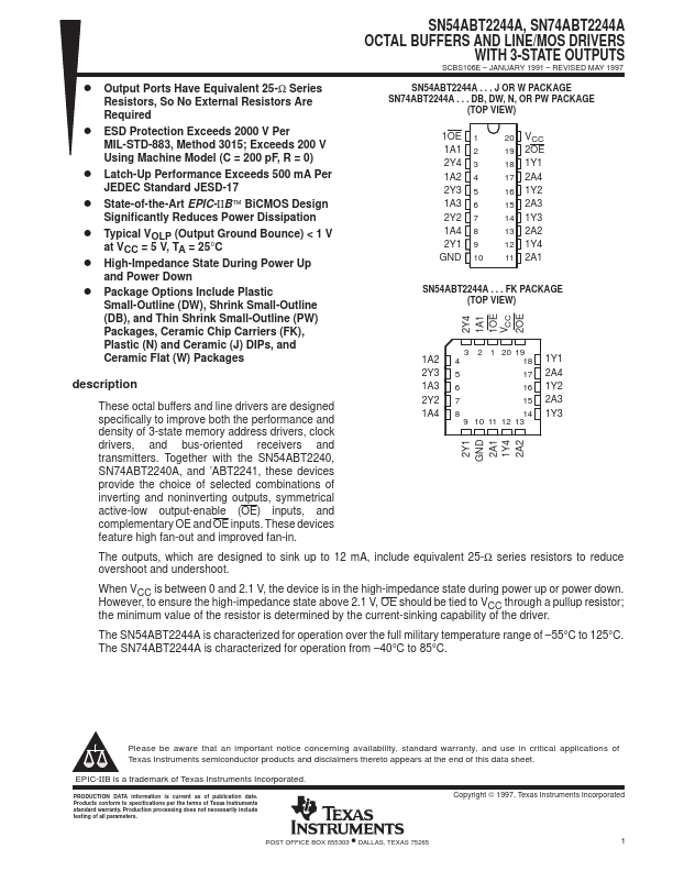
SN54ABT2244A . . . J OR W PACKAGE SN74ABT2244A . . . DB, DW, N, OR PW PACKAGE
(TOP VIEW)
1OE 1 1A1 2 2Y4 3 1A2 4 2Y3 5 1A3 6 2Y2 7 1A4 8 2Y1 9...