D State-of-the-Art EPIC-ΙΙB BiCMOS Design
Significantly Reduces Power Dissipation
D Latch-Up Performance Exceeds 500 mA...
D State-of-the-Art EPIC-ΙΙB Bi
CMOS Design
Significantly Reduces Power Dissipation
D Latch-Up Performance Exceeds 500 mA Per
JEDEC Standard JESD-17
D ESD Protection Exceeds 2000 V Per
MIL-STD-883, Method 3015; Exceeds 200 V Using Machine Model (C = 200 pF, R = 0)
D Typical VOLP (Output Ground Bounce) < 1 V
at VCC = 5 V, TA = 25°C
D High-Drive Outputs (−32-mA IOH, 64-mA IOL) D Package Options Include Plastic
Small-Outline (DW), Shrink Small-Outline (DB), and Thin Shrink Small-Outline (PW) Packages, Ceramic Chip Carriers (FK), Plastic (N) and Ceramic (J) DIPs, and Ceramic Flat (W) Package
SN54ABT244, SN74ABT244A OCTAL BUFFERS/DRIVERS WITH 3ĆSTATE OUTPUTS
SCBS099J − JANUARY 1991 − REVISED APRIL 2005
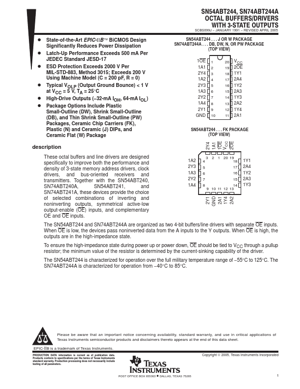
SN54ABT244 . . . J OR W PACKAGE SN74ABT244A . . . DB, DW, N, OR PW PACKAGE
(TOP VIEW)
1OE 1A1 2Y4 1A2 2Y3 1A3 2Y2 1A4 2Y1 GND
1 2 3 4 5 6 7 8 9 10
20 VCC 19 2OE 18 1Y1 17 2A4 16 1Y2 15 2A3 14 1Y3 13 2A2 12 1Y4 11 2A1
SN54ABT244 . . . FK PACKAGE (TOP VIEW)
2Y4 1A1 1OE VCC 2OE
description
These octal buffers and line drivers are designed
specifically to improve both the performance and
density of 3-state memory address drivers, clock
drivers, and bus-oriented receivers and
transmitters. Together with the SN54ABT240,
SN74ABT240A,
SN54ABT241,
and
SN74ABT241A, these devices provide the choice
of selected combinations of inverting and
noninverting outputs, symmetrical active-low
output-enable (OE) inputs, and complementary
OE and OE inputs.
2Y1 GND 2A1 1Y4 2A2
1A2
3 ...