D State-of-the-Art EPIC-ΙΙB™ BiCMOS Design
Significantly Reduces Power Dissipation
D ESD Protection Exceeds 2000 V Per
M...
D State-of-the-Art EPIC-ΙΙB™ Bi
CMOS Design
Significantly Reduces Power Dissipation
D ESD Protection Exceeds 2000 V Per
MIL-STD-883, Method 3015; Exceeds 200 V
Using Machine Model (C = 200 pF, R = 0)
D Latch-Up Performance Exceeds 500 mA Per
JEDEC Standard JESD-17
D Typical VOLP (Output Ground Bounce) < 1 V
at VCC = 5 V, TA = 25°C
D High-Drive Outputs (–32-mA IOH, 64-mA IOL) D Package Options Include Plastic
Small-Outline (DW), Shrink Small-Outline
(DB), and Thin Shrink Small-Outline (PW)
Packages, Ceramic Chip Carriers (FK),
Plastic (N) and Ceramic (J) DIPs, and
Ceramic Flat (W) Package
SN54ABT540, SN74ABT540 OCTAL BUFFERS/DRIVERS
WITH 3-STATE OUTPUTS
SCBS188C – FEBRUARY 1991 – REVISED JANUARY 1997
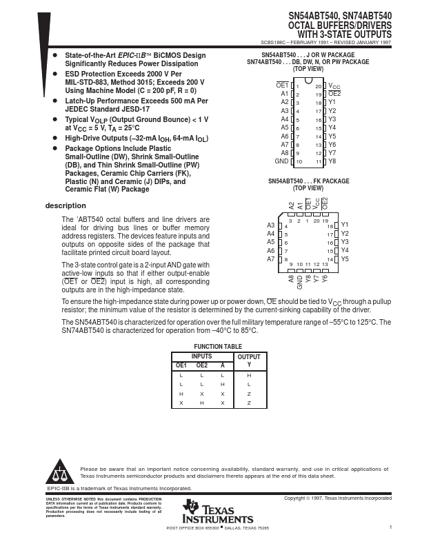
SN54ABT540 . . . J OR W PACKAGE SN74ABT540 . . . DB, DW, N, OR PW PACKAGE
(TOP VIEW)
OE1 1 A1 2 A2 3 A3 4 A4 5 A5 6 A6 7 A7 8 A8 9
GND 10
20 VCC 19 OE2 18 Y1 17 Y2 16 Y3 15 Y4 14 Y5 13 Y6 12 Y7 11 Y8
SN54ABT540 . . . FK PACKAGE (TOP VIEW)
A2 A1 OE1 VCC OE2
description
The ’ABT540 octal buffers and line drivers are ideal for driving bus lines or buffer memory address registers. The devices feature inputs and outputs on opposite sides of the package that facilitate printed circuit board layout.
The 3-state control gate is a 2-input AND gate with active-low inputs so that if either output-enable (OE1 or OE2) input is high, all corresponding outputs are in the high-impedance state.
A8 GND
Y8 Y7 Y6
A3
3 2 1 20 19
4
18
Y1
A4 5
17 Y2
A5 6
16 Y3
A6 7
15 Y4
A7 8
14 Y5
...