www.ti.com
FEATURES
• State-of-the-Art EPIC-IIB™ BiCMOS Design Significantly Reduces Power Dissipation
• Latch-Up Perfor...
www.ti.com
FEATURES
State-of-the-Art EPIC-IIB™ Bi
CMOS Design Significantly Reduces Power Dissipation
Latch-Up Performance Exceeds 500 mA Per JEDEC Standard JESD-17
Typical VOLP (Output Ground Bounce) < 1 V at VCC = 5 V, TA = 25°C
High-Impedance State During Power Up and Power Down
High-Drive Outputs (–32-mA IOH, 64-mA IOL) Package Options Include Plastic Small-Outline
(DW), Shrink Small-Outline (DB), and Thin Shrink Small-Outline (PW) Packages, Ceramic Chip Carriers (FK), Ceramic Flat (W) Package, and Plastic (N) and Ceramic (J) DIPs
SN54ABT541, SN74ABT541B OCTAL BUFFERS/DRIVERS
WITH 3-STATE OUTPUTS
SCBS093L – DECEMBER 1993 – REVISED DECEMBER 2006
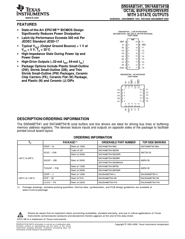
SN54ABT541...J OR W PACKAGE SN74ABT541B...DB, DW, N, OR PW PACKAGE
(TOP VIEW)
OE1 1 A1 2 A2 3 A3 4 A4 5 A5 6 A6 7 A7 8 A8 9
GND 10
20
V CC
19 OE2
18 Y1
17 Y2
16 Y3
15 Y4
14 Y5
13 Y6
12 Y7
11 Y8
SN54ABT541...FK PACKAGE (TOP VIEW)
A2 A1 OE1 V
CC
OE2
3 2 1 20 19
A3 4
18 Y1
A4 5
17 Y2
A5 6
16 Y3
A6 7
15 Y4
A7 8
14 Y5
9 10 11 12 13
A8 GND
Y8 Y7 Y6
DESCRIPTION/ORDERING INFORMATION
The SN54ABT541 and SN74ABT541B octal buffers and line drivers are ideal for driving bus lines or buffering memory address registers. The devices feature inputs and outputs on opposite sides of the package to facilitate printed circuit board layout.
TA –40°C to 85°C –55°C to 125°C
PDIP – N SOIC – DW
SSOP – DB
TSSOP – PW CDIP – J CFP – W LCCC – FK
ORDERING INFORMATION
PACKAGE (1)
ORDERABLE PART NUMBER
Reel of 1000
S...