D State-of-the-Art EPIC-ΙΙB™ BiCMOS Design
Significantly Reduces Power Dissipation
D ESD Protection Exceeds 2000 V Per
M...
D State-of-the-Art EPIC-ΙΙB™ Bi
CMOS Design
Significantly Reduces Power Dissipation
D ESD Protection Exceeds 2000 V Per
MIL-STD-883, Method 3015; Exceeds 200 V
Using Machine Model (C = 200 pF, R = 0)
D Latch-Up Performance Exceeds 500 mA Per
JEDEC Standard JESD-17
D Typical VOLP (Output Ground Bounce) < 1 V
at VCC = 5 V, TA = 25°C
D High-Drive Outputs (–32-mA IOH,
64-mA IOL )
D Package Options Include Plastic
Small-Outline (DW), Shrink Small-Outline
(DB), and Thin Shrink Small-Outline (PW)
Packages, Ceramic Chip Carriers (FK), and
Plastic (N) and Ceramic (J) DIPs
SN54ABT640, SN74ABT640 OCTAL BUS TRANSCEIVERS
WITH 3-STATE OUTPUTS
SCBS104C – FEBRUARY 1991 – REVISED JANUARY 1997
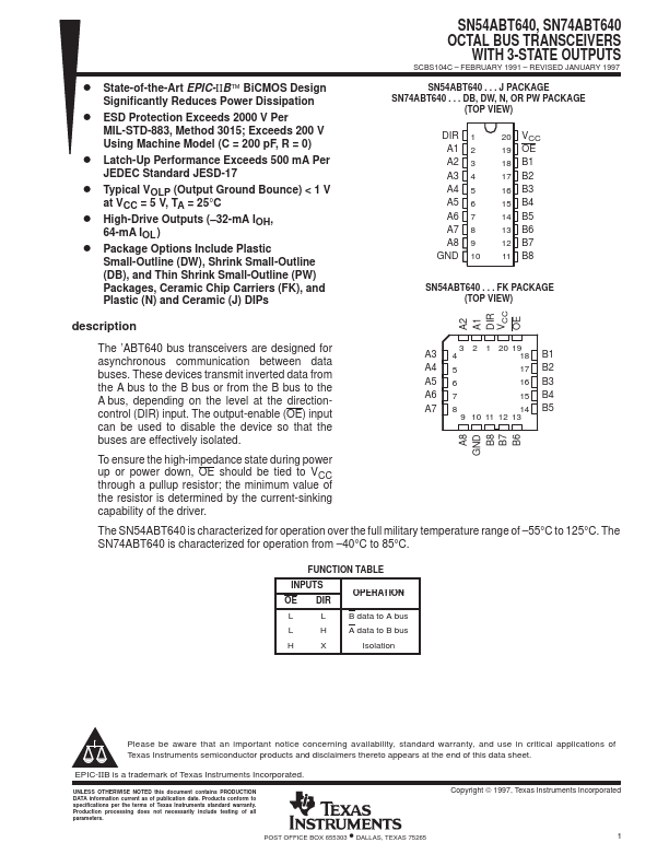
SN54ABT640 . . . J PACKAGE SN74ABT640 . . . DB, DW, N, OR PW PACKAGE
(TOP VIEW)
DIR 1 A1 2 A2 3 A3 4 A4 5 A5 6 A6 7 A7 8 A8 9
GND 10
20 VCC 19 OE 18 B1 17 B2 16 B3 15 B4 14 B5 13 B6 12 B7 11 B8
SN54ABT640 . . . FK PACKAGE (TOP VIEW)
OE
VCC
DIR
A1
A2
description
The ’ABT640 bus transceivers are designed for asynchronous communication between data buses. These devices transmit inverted data from the A bus to the B bus or from the B bus to the A bus, depending on the level at the directioncontrol (DIR) input. The output-enable (OE) input can be used to disable the device so that the buses are effectively isolated.
A3
3 2 1 20 19
4
18
B1
A4 5
17 B2
A5 6
16 B3
A6 7
15 B4
A7 8
14 B5
9 10 11 12 13
B6
B7
B8
GND
A8
To ensure the high-impedance state during power
up or power down, OE ...