SN54ABT651, SN74ABT651
OCTAL BUS TRANSCEIVERS AND REGISTERS WITH 3-STATE OUTPUTS
SCBS083E – JANUARY 1991 – REVISED APRIL...
SN54ABT651, SN74ABT651
OCTAL BUS TRANSCEIVERS AND REGISTERS WITH 3-STATE OUTPUTS
SCBS083E – JANUARY 1991 – REVISED APRIL 1998
D State-of-the-Art EPIC-ΙΙB™ Bi
CMOS Design
Significantly Reduces Power Dissipation
D ESD Protection Exceeds 2000 V Per
MIL-STD-883, Method 3015; Exceeds 200 V
Using Machine Model (C = 200 pF, R = 0)
D Latch-Up Performance Exceeds 500 mA Per
JESD 17
D Typical VOLP (Output Ground Bounce) < 1 V
at VCC = 5 V, TA = 25°C
D High-Drive Outputs (–32-mA IOH,
64-mA IOL )
D Multiplexed Real-Time and Stored Data D Inverting Data Paths D Package Options Include Plastic
Small-Outline (DW), Shrink Small-Outline
(DB), and Thin Shrink Small-Outline (PW)
Packages, Ceramic Chip Carriers (FK), and
Plastic (NT) and Ceramic (JT) DIPs
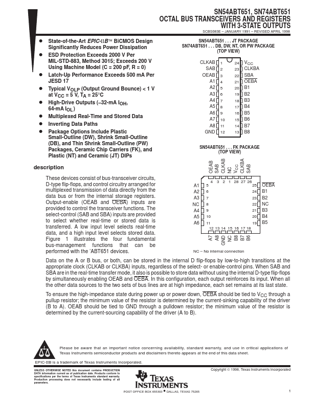
SN54ABT651 . . . JT PACKAGE SN74ABT651 . . . DB, DW, NT, OR PW PACKAGE
(TOP VIEW)
CLKAB 1 SAB 2
OEAB 3 A1 4 A2 5 A3 6 A4 7 A5 8 A6 9 A7 10 A8 11
GND 12
24 VCC 23 CLKBA 22 SBA 21 OEBA 20 B1 19 B2 18 B3 17 B4 16 B5 15 B6 14 B7 13 B8
SN54ABT651 . . . FK PACKAGE (TOP VIEW)
OEAB SAB CLKAB NC VCC CLKBA SAB
description
These devices consist of bus-transceiver circuits, D-type flip-flops, and control circuitry arranged for multiplexed transmission of data directly from the data bus or from the internal storage registers. Output-enable (OEAB and OEBA) inputs are provided to control the transceiver functions. The select-control (SAB and SBA) inputs are provided to select whether real-time or stored data is transferred. A low input level selects re...