SN54ABT657A, SN74ABT657A
OCTAL TRANSCEIVERS WITH PARITY GENERATORS/CHECKERS AND 3-STATE OUTPUTS
SCBS192E – JANUARY 1991 ...
SN54ABT657A, SN74ABT657A
OCTAL TRANSCEIVERS WITH PARITY GENERATORS/CHECKERS AND 3-STATE OUTPUTS
SCBS192E – JANUARY 1991 – REVISED JUNE 1997
D State-of-the-Art EPIC-ΙΙB™ Bi
CMOS Design
Significantly Reduces Power Dissipation
D ESD Protection Exceeds 2000 V Per
MIL-STD-883, Method 3015; Exceeds 200 V
Using Machine Model (C = 200 pF, R = 0)
D Latch-Up Performance Exceeds 500 mA Per
JEDEC Standard JESD-17
D Typical VOLP (Output Ground Bounce) < 1 V
at VCC = 5 V, TA = 25°C
D High-Impedance State During Power Up
and Power Down
D Flow-Through Architecture Optimizes PCB
Layout
D High-Drive Outputs (–32-mA IOH, 64-mA IOL) D Package Options Include Plastic
Small-Outline (DW) Packages, Ceramic
Chip Carriers (FK), and Plastic (NT) and
Ceramic (JT) DIPs
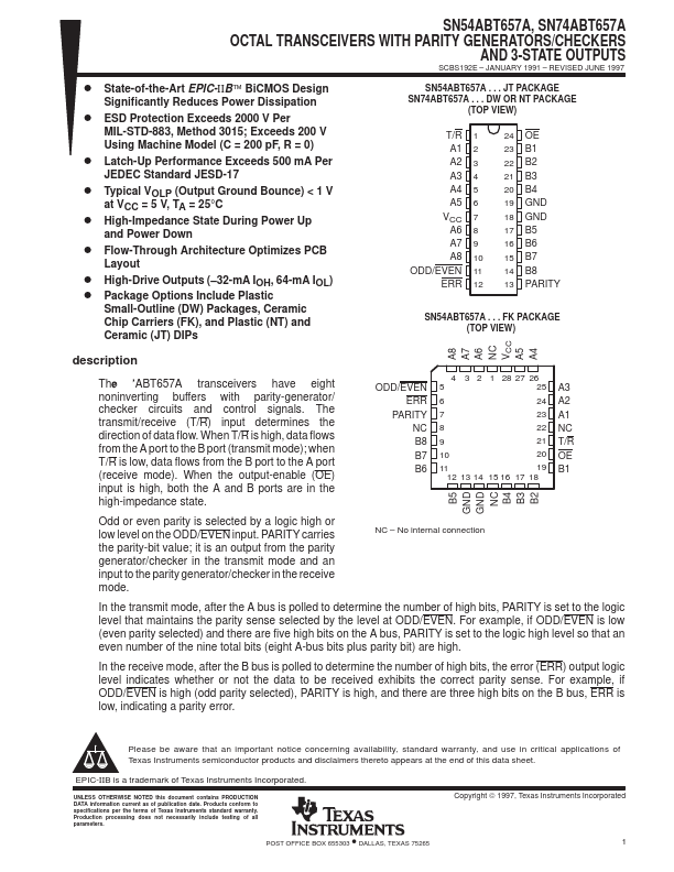
SN54ABT657A . . . JT PACKAGE SN74ABT657A . . . DW OR NT PACKAGE
(TOP VIEW)
T/R 1 A1 2 A2 3 A3 4 A4 5 A5 6 VCC 7 A6 8 A7 9 A8 10 ODD/EVEN 11 ERR 12
24 OE 23 B1 22 B2 21 B3 20 B4 19 GND 18 GND 17 B5 16 B6 15 B7 14 B8 13 PARITY
SN54ABT657A . . . FK PACKAGE (TOP VIEW)
A4
A5
VCC
NC
A6
A7
A8
description
The 'ABT657A transceivers have eight noninverting buffers with parity-generator/ checker circuits and control signals. The transmit/receive (T/R) input determines the direction of data flow. When T/R is high, data flows from the A port to the B port (transmit mode); when T/R is low, data flows from the B port to the A port (receive mode). When the output-enable (OE) input is high, both the A and B ports are in the high-impedance stat...