SN54ABTH18646A, SN54ABTH182646A, SN74ABTH18646A, SN74ABTH182646A
SCAN TEST DEVICES WITH 18-BIT TRANSCEIVERS AND REGISTER...
SN54ABTH18646A, SN54ABTH182646A, SN74ABTH18646A, SN74ABTH182646A
SCAN TEST DEVICES WITH 18-BIT TRANSCEIVERS AND REGISTERS
SCBS166D – AUGUST 1993 – REVISED JULY 1996
D Members of the Texas Instruments
SCOPE ™ Family of Testability Products
D Members of the Texas Instruments
Widebus ™ Family
D Compatible With the IEEE Standard
1149.1-1990 (JTAG) Test Access Port and
Boundary-Scan Architecture
D Include D-Type Flip-Flops and Control
Circuitry to Provide Multiplexed
Transmission of Stored and Real-Time Data
D Bus Hold on Data Inputs Eliminates the
Need for External Pullup Resistors
D B-Port Outputs of ’ABTH182646A Devices
Have Equivalent 25-Ω Series Resistors, So No External Resistors Are Required
D State-of-the-Art EPIC-ΙΙB ™ Bi
CMOS Design
D One Boundary-Scan Cell Per I/O
Architecture Improves Scan Efficiency
D SCOPE ™ Instruction Set
– IEEE Standard 1149.1-1990 Required Instructions and Optional CLAMP and HIGHZ
– Parallel-Signature Analysis at Inputs – Pseudo-Random Pattern Generation
From Outputs – Sample Inputs/Toggle Outputs – Binary Count From Outputs – Device Identification – Even-Parity Opcodes
D Packaged in 64-Pin Plastic Thin Quad Flat
(PM) Packages Using 0.5-mm Center-to-Center Spacings and 68-Pin Ceramic Quad Flat (HV) Packages Using 25-mil Center-to-Center Spacings
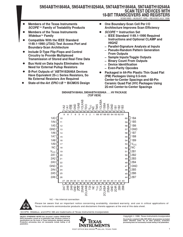
SN54ABTH18646A, SN54ABTH182646A . . . HV PACKAGE (TOP VIEW)
1A2 1A1 1OE GND 1SAB 1CLKAB TDO VCC NC TMS 1CLKBA 1SBA 1DIR GND 1B1 1B2 1B3
1A3 1A4 1A5 GND 1A6 1A7 1A8 1A9 NC VCC 2A1 2A2 2A3 GND 2A4 2A5 2...