SN54ABTH18502A, SN54ABTH182502A, SN74ABTH18502A, SN74ABTH182502A
SCAN TEST DEVICES WITH 18-BIT UNIVERSAL BUS TRANSCEIVER...
SN54ABTH18502A, SN54ABTH182502A, SN74ABTH18502A, SN74ABTH182502A
SCAN TEST DEVICES WITH 18-BIT UNIVERSAL BUS TRANSCEIVERS
SCBS164E – AUGUST 1993 – REVISED DECEMBER 1996
D Members of the Texas Instruments
SCOPE ™ Family of Testability Products
D Members of the Texas Instruments
Widebus ™ Family
D Compatible With the IEEE Standard
1149.1-1990 (JTAG) Test Access Port
and Boundary-Scan Architecture
D UBT ™ (Universal Bus Transceiver)
Combines D-Type Latches and D-Type
Flip-Flops for Operation in Transparent,
Latched, or Clocked Mode
D Bus Hold on Data Inputs Eliminates the
Need for External Pullup Resistors
D B-Port Outputs of ’ABTH182502A Devices
Have Equivalent 25-Ω Series Resistors, So No External Resistors Are Required
D State-of-the-Art EPIC-ΙΙB ™ Bi
CMOS Design
D One Boundary-Scan Cell Per I/O
Architecture Improves Scan Efficiency
D SCOPE Instruction Set
– IEEE Standard 1149.1-1990 Required Instructions and Optional CLAMP and HIGHZ
– Parallel-Signature Analysis at Inputs – Pseudo-Random Pattern Generation
From Outputs – Sample Inputs/Toggle Outputs – Binary Count From Outputs – Device Identification – Even-Parity Opcodes
D Packaged in 64-Pin Plastic Thin Quad Flat
(PM) Packages Using 0.5-mm Center-to-Center Spacings and 68-Pin Ceramic Quad Flat (HV) Packages Using 25-mil Center-to-Center Spacings
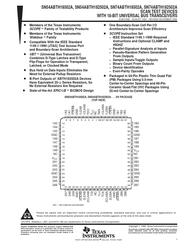
SN54ABTH18502A, SN54ABTH182502A . . . HV PACKAGE (TOP VIEW)
1A2 1A1 1OEAB GND 1LEAB 1CLKAB TDO VCC NC TMS 1CLKBA 1LEBA 1OEBA GND 1B1 1B2 1B3
1A3 1A4 1A5 GND 1A6 1A7 1A8 1A9 NC ...