SN54ABTR2245, SN74ABTR2245
OCTAL TRANSCEIVERS AND LINE/MEMORY DRIVERS WITH 3-STATE OUTPUTS
SCBS680A – MARCH 1997 – REVIS...
SN54ABTR2245, SN74ABTR2245
OCTAL TRANSCEIVERS AND LINE/MEMORY DRIVERS WITH 3-STATE OUTPUTS
SCBS680A – MARCH 1997 – REVISED MAY 1997
D Outputs Have Equivalent 25-Ω Series
Resistors, So No External Resistors Are Required
D State-of-the-Art EPIC-ΙΙB™ Bi
CMOS Design
Significantly Reduces Power Dissipation
D High-Impedance State During Power Up
and Power Down
D Latch-Up Performance Exceeds 500 mA Per
JEDEC Standard JESD-17
D ESD Protection Exceeds 2000 V Per
MIL-STD-833, Method 3015; Exceeds 200 V Using Machine Model (C = 200 pF, R = 0)
D Typical VOLP (Output Ground Bounce) < 1 V
at VCC = 5 V, TA = 25°C
D Package Options Include Plastic
Small-Outline (DW), Shrink Small-Outline (DB), Thin Shrink Small-Outline (PW), and Thin Very Small-Outline (DGV) Packages, Ceramic Chip Carriers (FK), and Plastic (N) and Ceramic (J) DIPs
description
These octal transceivers and line drivers are designed for asynchronous communication between data buses. The devices transmit data from the A bus to the B bus or from the B bus to the A bus, depending on the logic level at the direction-control (DIR) input. The output-enable (OE) input can be used to disable the device so the buses are effectively isolated.
A8
GND
B8
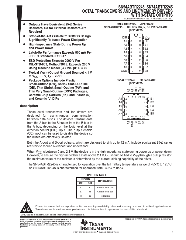
SN54ABTR2245 . . . J PACKAGE SN74ABTR2245 . . . DB, DGV, DW, N, OR PW PACKAGE
(TOP VIEW)
DIR 1 A1 2 A2 3 A3 4 A4 5 A5 6 A6 7 A7 8 A8 9
GND 10
20 VCC 19 OE 18 B1 17 B2 16 B3 15 B4 14 B5 13 B6 12 B7 11 B8
SN54ABTR2245 . . . FK PACKAGE (TOP VIEW)
OE
VC C
DIR
A1
A2
A3
3 2 1 20 1...