SN74AC240ĆQ1 OCTAL BUFFER/DRIVER WITH 3ĆSTATE OUTPUTS
SCAS785A − OCTOBER 2004 − REVISED JANUARY 2008
D Qualified for Au...
SN74AC240ĆQ1 OCTAL BUFFER/DRIVER WITH 3ĆSTATE OUTPUTS
SCAS785A − OCTOBER 2004 − REVISED JANUARY 2008
D Qualified for Automotive Applications D 2-V to 6-V VCC Operation D Inputs Accept
Voltages to 6 V D Max tpd of 6.5 ns at 5 V
description/ordering information
This octal buffer and line driver is designed specifically to improve the performance and density of 3-state memory address drivers, clock drivers, and bus-oriented receivers and transmitters.
The SN74AC240 device is organized as two 4-bit buffers/drivers with separate output-enable (OE) inputs. When OE is low, the device passes inverted data from the A inputs to the Y outputs. When OE is high, the outputs are in the high-impedance state.
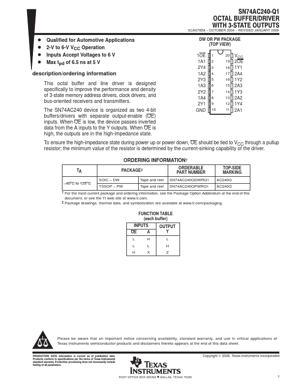
DW OR PW PACKAGE (TOP VIEW)
1OE 1 1A1 2 2Y4 3 1A2 4 2Y3 5 1A3 6 2Y2 7 1A4 8 2Y1 9 GND 10
20 VCC 19 2OE 18 1Y1 17 2A4 16 1Y2 15 2A3 14 1Y3 13 2A2 12 1Y4 11 2A1
To ensure the high-impedance state during power up or power down, OE should be tied to VCC through a pullup resistor; the minimum value of the resistor is determined by the current-sinking capability of the driver.
ORDERING INFORMATION†
TA
PACKAGE‡
ORDERABLE PART NUMBER
TOP-SIDE MARKING
−40°C to 125°C
SOIC − DW TSSOP − PW
Tape and reel SN74AC240QDWRQ1 Tape and reel SN74AC240QPWRQ1
AC240Q AC240Q
† For the most current package and ordering information, see the Package Option Addendum at the end of this
document, or see the TI web site at www.ti.com. ‡ Package drawings, thermal data, and symbolization are available at ...