D 2-V to 6-V VCC Operation D Inputs Accept Voltages to 6 V D Max tpd of 7.5 ns at 5 V
description/ordering information
T...
D 2-V to 6-V VCC Operation D Inputs Accept
Voltages to 6 V D Max tpd of 7.5 ns at 5 V
description/ordering information
These octal buffers and line drivers are designed specifically to improve the performance and density of 3-state memory address drivers, clock drivers, and bus-oriented receivers and transmitters.
The ’AC241 devices are organized as two 4-bit buffers/drivers with separate complementary output-enable (1OE and 2OE) inputs. When 1OE is low or 2OE is high, the device passes noninverted data from the A inputs to the Y outputs. When 1OE is high or 2OE is low, the outputs are in the high-impedance state.
To ensure the high-impedance state during power up or power down, OE should be tied to VCC through a pullup resistor and OE should be tied to GND through a pulldown resistor; the minimum value of the resistor is determined by the current-sinking or the current-sourcing capability of the driver.
SN54AC241, SN74AC241 OCTAL BUFFERS/DRIVERS
WITH 3-STATE OUTPUTS
SCAS513E − JUNE 1995 − REVISED OCTOBER 2003
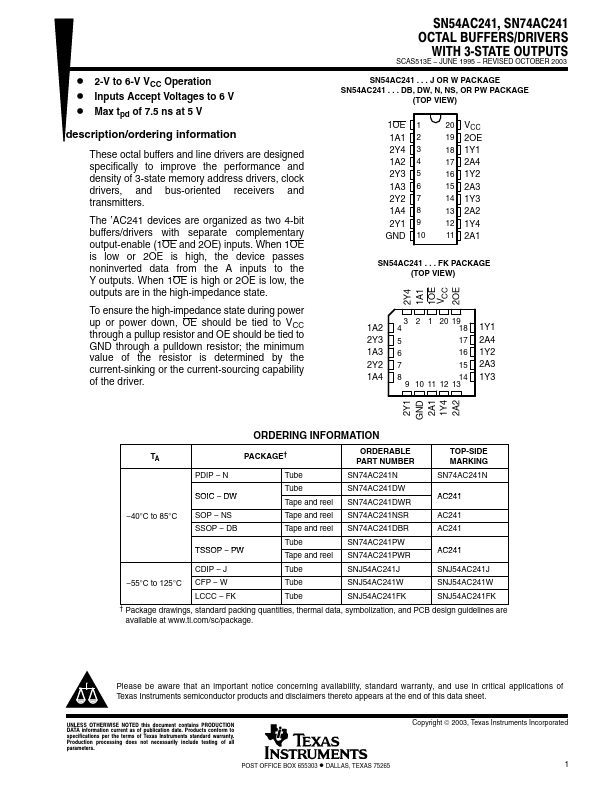
SN54AC241 . . . J OR W PACKAGE SN54AC241 . . . DB, DW, N, NS, OR PW PACKAGE
(TOP VIEW)
1OE 1 1A1 2 2Y4 3 1A2 4 2Y3 5 1A3 6 2Y2 7 1A4 8 2Y1 9 GND 10
20 VCC 19 2OE 18 1Y1 17 2A4 16 1Y2 15 2A3 14 1Y3 13 2A2 12 1Y4 11 2A1
SN54AC241 . . . FK PACKAGE (TOP VIEW)
2Y4 1A1 1OE VCC 2OE
3 2 1 20 19
1A2 4
18 1Y1
2Y3 5
17 2A4
1A3 6
16 1Y2
2Y2 7
15 2A3
1A4 8
14 1Y3
9 10 11 12 13
2Y1 GND 2A1 1Y4 2A2
ORDERING INFORMATION
TA
PACKAGE†
ORDERABLE PART NUMBER
TOP-SIDE ...