D Q Devices Meet Automotive Performance
Requirements
D Customer-Specific Configuration Control
Can Be Supported Along Wi...
D Q Devices Meet Automotive Performance
Requirements
D Customer-Specific Configuration Control
Can Be Supported Along With Major-Change Approval
D EPIC (Enhanced-Performance Implanted
CMOS) Process
D Operating Range 2-V to 5.5-V VCC D Latch-Up Performance Exceeds 250 mA Per
JESD 17
description
SN74AHC244Q OCTAL BUFFER/DRIVER WITH 3-STATE OUTPUTS
SGDS017 – FEBRUARY 2002
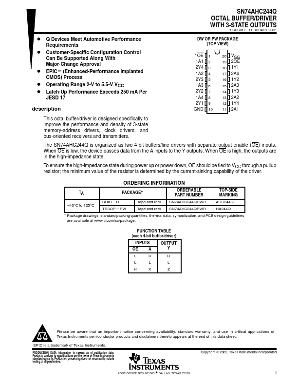
DW OR PW PACKAGE (TOP VIEW)
1OE 1A1 2Y4 1A2 2Y3 1A3 2Y2 1A4 2Y1 GND
1 2 3 4 5 6 7 8 9 10
20 VCC 19 2OE 18 1Y1 17 2A4 16 1Y2 15 2A3 14 1Y3 13 2A2 12 1Y4 11 2A1
This octal buffer/driver is designed specifically to improve the performance and density of 3-state memory-address drivers, clock drivers, and bus-oriented receivers and transmitters.
The SN74AHC244Q is organized as two 4-bit buffers/line drivers with separate output-enable (OE) inputs. When OE is low, the device passes data from the A inputs to the Y outputs. When OE is high, the outputs are in the high-impedance state.
To ensure the high-impedance state during power up or power down, OE should be tied to VCC through a pullup resistor; the minimum value of the resistor is determined by the current-sinking capability of the driver.
ORDERING INFORMATION
TA
PACKAGE†
ORDERABLE PART NUMBER
TOP-SIDE MARKING
–40°C to 125°C
SOIC – D TSSOP – PW
Tape and reel Tape and reel
SN74AHC244QDWR SN74AHC244QPWR
AHC244Q HA244Q
† Package drawings, standard packing quantities, thermal data, symbolization, and PCB design guidelines are available at www.ti.co...