SN54ALS109A, SN54AS109A, SN74ALS109A, SN74AS109A DUAL JĆK POSITIVEĆEDGEĆTRIGGERED FLIPĆFLOPS WITH CLEAR AND PRESET
SDAS1...
SN54ALS109A, SN54AS109A, SN74ALS109A, SN74AS109A DUAL JĆK POSITIVEĆEDGEĆTRIGGERED FLIPĆFLOPS WITH CLEAR AND PRESET
SDAS198B − APRIL 1982 − REVISED AUGUST 1995
Package Options Include Plastic
Small-Outline (D) Packages, Ceramic Chip Carriers (FK), and Standard Plastic (N) and Ceramic (J) 300-mil DIPs
TYPE
′ALS109A ′AS109A
TYPICAL MAXIMUM CLOCK
FREQUENCY (MHz)
50
129
TYPICAL POWER DISSIPATION
PER FLIP-FLOP (mW)
6
29
description
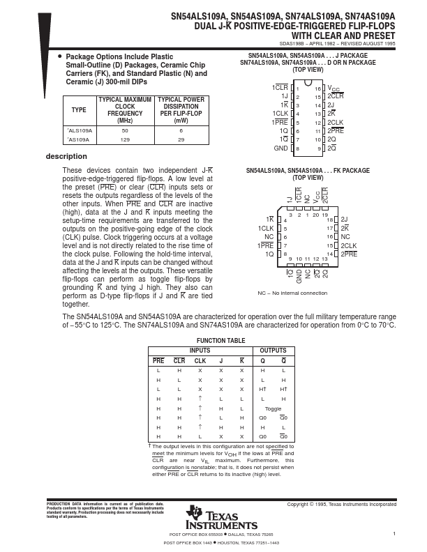
SN54ALS109A, SN54AS109A . . . J PACKAGE SN74ALS109A, SN74AS109A . . . D OR N PACKAGE
(TOP VIEW)
1CLR 1 1J 2 1K 3
1CLK 4 1PRE 5
1Q 6 1Q 7 GND 8
16 VCC 15 2CLR 14 2J 13 2K 12 2CLK 11 2PRE 10 2Q 9 2Q
These devices contain two independent J-K positive-edge-triggered flip-flops. A low level at the preset (PRE) or clear (CLR) inputs sets or resets the outputs regardless of the levels of the other inputs. When PRE and CLR are inactive (high), data at the J and K inputs meeting the setup-time requirements are transferred to the outputs on the positive-going edge of the clock (CLK) pulse. Clock triggering occurs at a
voltage level and is not directly related to the rise time of the clock pulse. Following the hold-time interval, data at the J and K inputs can be changed without affecting the levels at the outputs. These versatile flip-flops can perform as toggle flip-flops by grounding K and tying J high. They also can perform as D-type flip-flops if J and K are tied together.
SN54ALS109A, SN54AS109A . . . FK PACKAGE (TOP VIEW)
1J 1CLR NC VCC 2CLR
1K...