4-Bit Bidirectional Universal Shift Register
ą
SN54AS194, SN74AS194
4ĆBIT BIDIRECTIONAL UNIVERSAL SHIFT REGISTERS
ą
SDAS212A − DECEMBER 1983 − REVISED DECEMBER 1...
Description
ą
SN54AS194, SN74AS194
4ĆBIT BIDIRECTIONAL UNIVERSAL SHIFT REGISTERS
ą
SDAS212A − DECEMBER 1983 − REVISED DECEMBER 1994
Parallel-to-Serial, Serial-to-Parallel
Conversions
Left or Right Shifts Parallel Synchronous Loading Direct Overriding Clear Temporary Data-Latching Capability Package Options Include Plastic
Small-Outline Packages (D), Ceramic Chip
Carriers (FK), and Standard Plastic (N) and
Ceramic (J) 300-mil DIPs
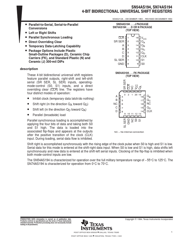
SN54AS194 . . . J PACKAGE SN74AS194 . . . D OR N PACKAGE
(TOP VIEW)
CLR 1 SR SER 2
A3 B4 C5 D6 SL SER 7 GND 8
16 VCC 15 QA 14 QB 13 QC 12 QD 11 CLK
10 S1
9 S0
description
These 4-bit bidirectional universal shift registers feature parallel outputs, right-shift and left-shift serial (SR SER, SL SER) inputs, operatingmode-control (S0, S1) inputs, and a direct overriding clear (CLR) line. The registers have four distinct modes of operation:
Inhibit clock (temporary data latch/do nothing) Shift right (in the direction QA toward QD) Shift left (in the direction QD toward QA) Parallel (broadside) load
SN54AS194 . . . FK PACKAGE (TOP VIEW)
SR SER CLR NC VCC QA
A
3 2 1 20 19
4
18
QB
B5
17 QC
NC 6
16 NC
C7
15 QD
D8
14 CLK
9 10 11 12 13
SL SER GND NC S0 S1
Parallel synchronous loading is accomplished by applying the four bits of data and taking both S0 and S1 high. The data is loaded into the associated flip-flops and appears at the outputs after the positive transition of the clock (CLK) input. During loading, serial data fl...
Similar Datasheet