QUADRUPLE 2-INPUT POSITIVE-NOR GATE
www.ti.com
FEATURES
• Optimized for 1.8-V Operation and Is 3.6-V I/O Tolerant to Support Mixed-Mode Signal Operation
• I...
Description
www.ti.com
FEATURES
Optimized for 1.8-V Operation and Is 3.6-V I/O Tolerant to Support Mixed-Mode Signal Operation
Ioff Supports Partial-Power-Down Mode Operation
Sub-1-V Operable Max tpd of 2.2 ns at 1.8 V Low Power Consumption, 10-µA Max ICC ±8-mA Output Drive at 1.8 V Latch-Up Performance Exceeds 100 mA Per
JESD 78, Class II ESD Protection Exceeds JESD 22
– 2000-V Human-Body Model (A114-A) – 200-V Machine Model (A115-A) – 1000-V Charged-Device Model (C101)
GND
SN74AUC02 QUADRUPLE 2-INPUT POSITIVE-NOR GATE
SCES511A – NOVEMBER 2003 – REVISED MARCH 2005
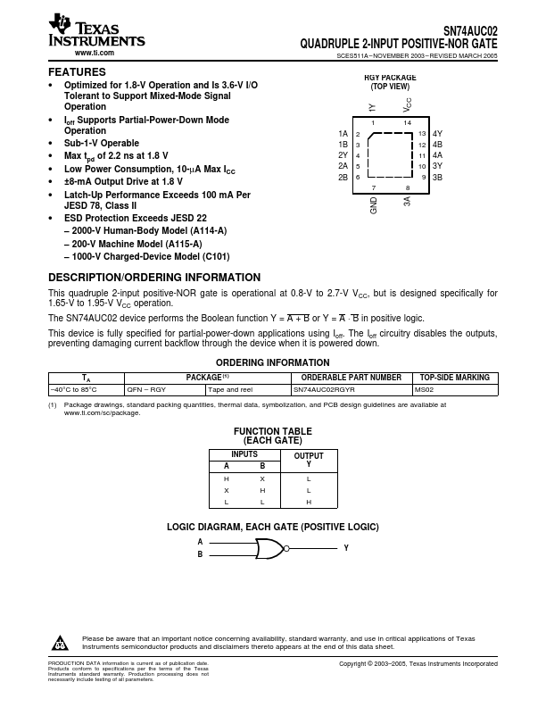
RGY PACKAGE (TOP VIEW)
VCC
1Y
1 1A 2 1B 3 2Y 4 2A 5 2B 6
7
14 13 4Y 12 4B 11 4A 10 3Y 9 3B
8
3A
DESCRIPTION/ORDERING INFORMATION
This quadruple 2-input positive-NOR gate is operational at 0.8-V to 2.7-V VCC, but is designed specifically for 1.65-V to 1.95-V VCC operation.
The SN74AUC02 device performs the Boolean function Y = A + B or Y = A ⋅ B in positive logic.
This device is fully specified for partial-power-down applications using Ioff. The Ioff circuitry disables the outputs, preventing damaging current backflow through the device when it is powered down.
TA –40°C to 85°C
QFN – RGY
ORDERING INFORMATION
PACKAGE (1)
ORDERABLE PART NUMBER
Tape and reel
SN74AUC02RGYR
TOP-SIDE MARKING MS02
(1) Package drawings, standard packing quantities, thermal data, symbolization, and PCB design guidelines are available at www.ti.com/sc/package.
FUNCTION TABLE (EACH GATE)
INPUTS
A
B
H
X
X
H
L
L
O...
Similar Datasheet