www.ti.com
SN74AUC1G80 SINGLE POSITIVE-EDGE-TRIGGERED D-TYPE FLIP-FLOP
SCES388K – MARCH 2002 – REVISED JANUARY 2007
FE...
www.ti.com
SN74AUC1G80 SINGLE POSITIVE-EDGE-TRIGGERED D-TYPE FLIP-FLOP
SCES388K – MARCH 2002 – REVISED JANUARY 2007
FEATURES
Available in the Texas Instruments NanoFree™ Package
Optimized for 1.8-V Operation and Is 3.6-V I/O Tolerant to Support Mixed-Mode Signal Operation
Ioff Supports Partial-Power-Down Mode Operation
Sub-1-V Operable Max tpd of 1.9 ns at 1.8 V
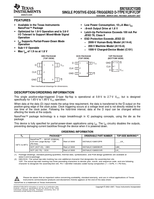
DBV PACKAGE (TOP VIEW)
Low Power Consumption, 10-µA Max ICC ±8-mA Output Drive at 1.8 V Latch-Up Performance Exceeds 100 mA Per
JESD 78, Class II ESD Protection Exceeds JESD 22
– 2000-V Human-Body Model (A114-A)
– 200-V Machine Model (A115-A)
– 1000-V Charged-Device Model (C101)
DCK PACKAGE (TOP VIEW)
YZP PACKAGE (BOTTOM VIEW)
D
1
CLK
2
5
VCC
D
1
5
VCC
CLK
2
GND
3
4Q
GND 3 4 Q CLK 2
D 1 5 VCC
GND
3
4
Q
See mechanical drawings for dimensions.
DESCRIPTION/ORDERING INFORMATION
This single positive-edge-triggered D-type flip-flop is operational at 0.8-V to 2.7-V VCC, but is designed specifically for 1.65-V to 1.95-V VCC operation.
When data at the data (D) input meets the setup time requirement, the data is transferred to the Q output on the positive-going edge of the clock pulse. Clock triggering occurs at a
voltage level and is not directly related to the rise time of the clock pulse. Following the hold-time interval, data at the D input can be changed without affecting the levels at the outputs.
NanoFree™ package technology is a major breakthrough in IC packaging concepts, ...