Dual Buffer/Driver
SN74AUC2G07
www.ti.com....................................................................................................
Description
SN74AUC2G07
www.ti.com............................................................................................................................................................... SCES443D – MAY 2003 – REVISED JUNE 2008
DUAL BUFFER/DRIVER WITH OPEN-DRAIN OUTPUTS
FEATURES
1
2 Available in the Texas Instruments NanoFree™ Package
Optimized for 1.8-V Operation and Is 3.6-V I/O Tolerant to Support Mixed-Mode Signal Operation
Ioff Supports Partial-Power-Down Mode Operation
Sub-1-V Operable Max tpd of 2.5 ns at 1.8 V
Low Power Consumption, 10 µA at 1.8 V ±8-mA Output Drive at 1.8 V Latch-Up Performance Exceeds 100 mA Per
JESD 78, Class II ESD Protection Exceeds JESD 22
– 2000-V Human-Body Model (A114-A)
– 200-V Machine Model (A115-A)
– 1000-V Charged-Device Model (C101)
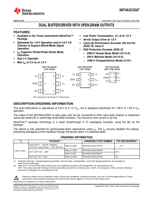
DBV PACKAGE (TOP VIEW)
DCK PACKAGE (TOP VIEW)
YZP PACKAGE (BOTTOM VIEW)
1A GND
1 2
1A 1 6 1Y
2A 3 4 2Y
6 1Y
GND 2 5 VCC
GND 2 5 VCC
1A 1 6 1Y
5 VCC 2A 3 4 2Y
2A 3
4 2Y
See mechanical drawings for dimensions.
DESCRIPTION/ORDERING INFORMATION
This dual buffer/driver is operational at 0.8-V to 2.7-V VCC, but is designed specifically for 1.65-V to 1.95-V VCC operation.
The output of the SN74AUC2G07 is open drain and can be connected to other open-drain outputs to implement active-low wired-OR or active-high wired-AND functions. The maximum sink current is 32 mA.
NanoFree™ package technology is a major breakthrough in IC packaging concepts, using the die as the package.
This device is...
Similar Datasheet