DUAL BUS BUFFER GATE
www.ti.com
SN74AUC2G125 DUAL BUS BUFFER GATE WITH 3-STATE OUTPUTS
SCES532D – DECEMBER 2003 – REVISED AUGUST 2007
FEATU...
Description
www.ti.com
SN74AUC2G125 DUAL BUS BUFFER GATE WITH 3-STATE OUTPUTS
SCES532D – DECEMBER 2003 – REVISED AUGUST 2007
FEATURES
Available in the Texas Instruments NanoFree™ Package
Optimized for 1.8-V Operation and Is 3.6-V I/O Tolerant to Support Mixed-Mode Signal Operation
Ioff Supports Partial-Power-Down Mode Operation
Sub-1-V Operable
Max tpd of 1.8 ns at 1.8 V
Low Power Consumption, 10 μA at 1.8 V ±8-mA Output Drive at 1.8 V Latch-Up Performance Exceeds 100 mA Per
JESD 78, Class II ESD Protection Exceeds JESD 22
– 2000-V Human-Body Model (A114-A)
– 200-V Machine Model (A115-A)
– 1000-V Charged-Device Model (C101)
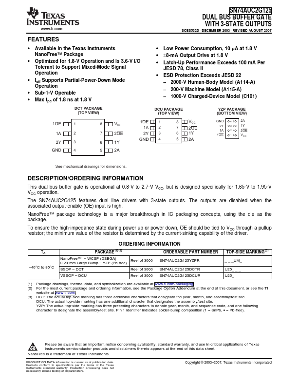
DCT PACKAGE (TOP VIEW)
DCU PACKAGE (TOP VIEW)
YZP PACKAGE (BOTTOM VIEW)
1OE 1A 2Y
1 2 3
8 VCC 7 2OE 6 1Y
1OE 1A 2Y
GND
1 2 3 4
8 VCC 7 2OE 6 1Y
5 2A
GND 4 5 2A 2Y 3 6 1Y 1A 2 7 2OE
1OE 1 8 VCC
GND
4
5 2A
See mechanical drawings for dimensions.
DESCRIPTION/ORDERING INFORMATION
This dual bus buffer gate is operational at 0.8-V to 2.7-V VCC, but is designed specifically for 1.65-V to 1.95-V VCC operation.
The SN74AUC2G125 features dual line drivers with 3-state outputs. The outputs are disabled when the associated output-enable (OE) input is high.
NanoFree™ package technology is a major breakthrough in IC packaging concepts, using the die as the package.
To ensure the high-impedance state during power up or power down, OE should be tied to VCC through a pullup resistor; the minimum value of the resistor is determined by the current-si...
Similar Datasheet