www.ti.com
SN74AVC24T245 SCES552E – FEBRUARY 2004 – RESVNIS7E4DAAVUCGU2S4TT2204250
SCES552E – FEBRUARY 2004 – REVISED A...
www.ti.com
SN74AVC24T245 SCES552E – FEBRUARY 2004 – RESVNIS7E4DAAVUCGU2S4TT2204250
SCES552E – FEBRUARY 2004 – REVISED AUGUST 2020
24-Bit Dual-Supply Bus Transceiver with Configurable
Voltage Translation And 3-
State Outputs
1 Features
Control Inputs VIH/VIL Levels Are Referenced to VCCA
Voltage
VCC Isolation Feature – If Either VCC Input Is at GND, All Outputs Are in the High-Impedance State
Over
voltage-Tolerant Inputs/Outputs Allow Mixed
Voltage-Mode Data Communications
Fully Configurable Dual-Rail Design Allows Each Port to Operate Over Full 1.2-V to 3.6-V PowerSupply Range
Ioff Supports Partial-Power-Down Mode Operation I/Os Are 4.6-V Tolerant Max Data Rates
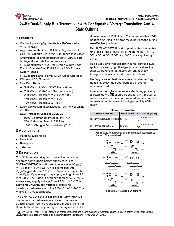
– 380 Mbps (1.8-V to 3.3-V Translation) – 200 Mbps (<1.8-V to 3.3-V Translation) – 200 Mbps (Translate to 2.5 V or 1.8 V) – 150 Mbps (Translate to 1.5 V) – 100 Mbps (Translate to 1.2 V) Latch-Up Performance Exceeds 100 mA Per JESD 78, Class II ESD Protection Exceeds JESD 22 – 8000-V Human-Body Model (A114-A) – 200-V Machine Model (A115-A) – 1000-V Charged-Device Model (C101)
2 Applications
Personal Electronics Industrial Enterprise Telecom
3 Description
This 24-bit noninverting bus transceiver uses two separate configurable power-supply rails. The SN74AVC24T245 is optimized to operate with VCCA/ VCCB set at 1.4 V to 3.6 V. It is operational with VCCA/VCCB as low as 1.2 V. The A port is designed to track VCCA. VCCA accepts any supply
voltage from 1.2 V to 3.6 V. The B port is designed to tra...