D Operating Voltage Range of 4.5 V to 5.5 V D State-of-the-Art BiCMOS Design
Significantly Reduces ICCZ
SN54BCT125A . . ...
D Operating
Voltage Range of 4.5 V to 5.5 V D State-of-the-Art Bi
CMOS Design
Significantly Reduces ICCZ
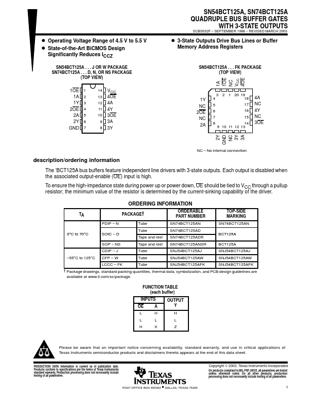
SN54BCT125A . . . J OR W PACKAGE SN74BCT125A . . . D, N, OR NS PACKAGE
(TOP VIEW)
1OE 1 1A 2 1Y 3
2OE 4 2A 5 2Y 6
GND 7
14 VCC 13 4OE 12 4A 11 4Y 10 3OE 9 3A 8 3Y
SN54BCT125A, SN74BCT125A QUADRUPLE BUS BUFFER GATES
WITH 3-STATE OUTPUTS
SCBS032F – SEPTEMBER 1988 – REVISED MARCH 2003
D 3-State Outputs Drive Bus Lines or Buffer
Memory Address Registers
SN54BCT125A . . . FK PACKAGE (TOP VIEW)
1A 1OE NC VCC 4OE
1Y NC 2OE NC 2A
3 2 1 20 19
4
18
5
17
6
16
7
15
8
14
9 10 11 12 13
4A NC 4Y NC 3OE
2Y GND
NC 3Y 3A
NC – No internal connection
description/ordering information
The ’BCT125A bus buffers feature independent line drivers with 3-state outputs. Each output is disabled when the associated output-enable (OE) input is high.
To ensure the high-impedance state during power up or power down, OE should be tied to VCC through a pullup resistor; the minimum value of the resistor is determined by the current-sinking capability of the driver.
ORDERING INFORMATION
TA
PACKAGE†
ORDERABLE PART NUMBER
TOP-SIDE MARKING
PDIP – N
Tube
SN74BCT125AN
SN74BCT125AN
0°C to 70°C
SOIC – D
Tube Tape and reel
SN74BCT125AD SN74BCT125ADR
BCT125A
SOP – NS
Tape and reel SN74BCT125ANSR
BCT125A
CDIP – J
Tube
SNJ54BCT125AJ
SNJ54BCT125AJ
–55°C to 125°C CFP – W
Tube
SNJ54BCT125AW
SNJ54BCT125AW
LCCC – FK
Tube
SNJ54BCT125AFK
SNJ54BCT125AFK
† Package drawings, standar...