• State-of-the-Art BiCMOS Design
Significantly Reduces ICCZ
• ESD Protection Exceeds 2000 V Per
MIL-STD-883C, Method 301...
State-of-the-Art Bi
CMOS Design
Significantly Reduces ICCZ
ESD Protection Exceeds 2000 V Per
MIL-STD-883C, Method 3015; Exceeds 200 V Using Machine Model (C = 200 pF, R = 0)
3-State Outputs Drive Bus Lines or Buffer
Memory Address Registers
P-N-P Inputs Reduce DC Loading Flow-Through Architecture Optimizes
PCB Layout
Package Options Include Plastic
Small-Outline (DW) Packages, Ceramic Chip Carriers (FK) and Flatpacks (W), and Standard Plastic and Ceramic 300-mil DIPs (JT, NT)
description
These 10-bit buffers and bus drivers provide high-performance bus interface for wide data paths or buses carrying parity.
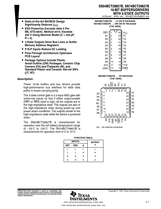
The 3-state control gate is a 2-input AND gate with active-low inputs so that if either output-enable (OE1 or OE2) input is high, all ten outputs are in the high-impedance state. The outputs are also in the high-impedance state during power-up and power-down conditions. The outputs remain in the high-impedance state while the device is powered down.
The SN54BCT29827B is characterized for operation over the full military temperature range of − 55°C to 125°C. The SN74BCT29827B is characterized for operation from 0°C to 70°C.
SN54BCT29827B, SN74BCT29827B 10-BIT BUFFERS/DRIVERS WITH 3-STATE OUTPUTS
SCBS008C − APRIL 1987 − REVISED NOVEMBER 1993
SN54BCT29827B . . . JT OR W PACKAGE SN74BCT29827B . . . DW OR NT PACKAGE
(TOP VIEW)
OE1 1 A1 2 A2 3 A3 4 A4 5 A5 6 A6 7 A7 8 A8 9 A9 10
A10 11 GND 12
24 VCC 23 Y1 22 Y2 21 Y3 20 Y4 19 Y5 18 Y6 17 Y7 16 Y8 15 Y9 14 Y10 13 OE...