• State-of-the-Art BiCMOS Design
Significantly Reduces ICCZ
• ESD Protection Exceeds 2000 V Per
MIL-STD-883C, Method 301...
State-of-the-Art Bi
CMOS Design
Significantly Reduces ICCZ
ESD Protection Exceeds 2000 V Per
MIL-STD-883C, Method 3015; Exceeds
200 V Using Machine Model (C = 200 pF,
R = 0)
Independent Registers and Enables for
A and B Buses
Multiplexed Real-Time and Stored Data Power-Up High-Impedance Mode Package Options Include Plastic
Small-Outline (DW) Packages, Ceramic
Chip Carriers (FK) and Flatpacks (W), and
Standard Plastic and Ceramic 300-mil DIPs
(JT, NT)
SN54BCT652, SN74BCT652 OCTAL BUS TRANSCEIVERS AND REGISTERS
WITH 3-STATE OUTPUTS
SCBS038A − AUGUST 1989 − REVISED NOVEMBER 1993
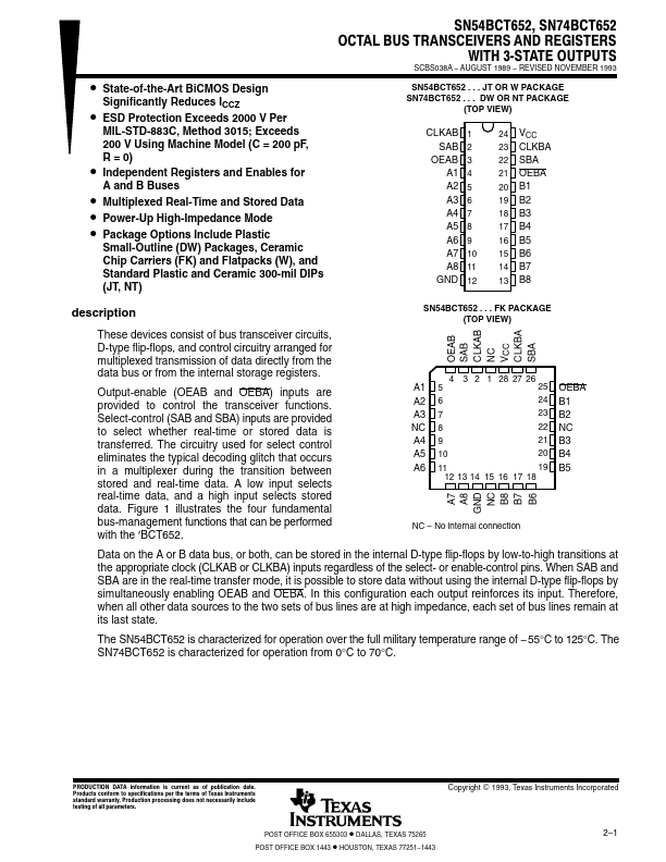
SN54BCT652 . . . JT OR W PACKAGE SN74BCT652 . . . DW OR NT PACKAGE
(TOP VIEW)
CLKAB 1 SAB 2
OEAB 3 A1 4 A2 5 A3 6 A4 7 A5 8 A6 9 A7 10 A8 11
GND 12
24 VCC 23 CLKBA 22 SBA 21 OEBA 20 B1 19 B2 18 B3 17 B4 16 B5 15 B6 14 B7 13 B8
description
These devices consist of bus transceiver circuits, D-type flip-flops, and control circuitry arranged for multiplexed transmission of data directly from the data bus or from the internal storage registers.
Output-enable (OEAB and OEBA) inputs are provided to control the transceiver functions. Select-control (SAB and SBA) inputs are provided to select whether real-time or stored data is transferred. The circuitry used for select control eliminates the typical decoding glitch that occurs in a multiplexer during the transition between stored and real-time data. A low input selects real-time data, and a high input selects stored data. Figure 1 illustrates the ...