SN74CB3T16210
www.ti.com
SCDS156B – OCTOBER 2003 – REVISED JULY 2012
20-BIT FET BUS SWITCH 2.5-V/3.3-V LOW-VOLTAGE BU...
SN74CB3T16210
www.ti.com
SCDS156B – OCTOBER 2003 – REVISED JULY 2012
20-BIT FET BUS SWITCH 2.5-V/3.3-V LOW-
VOLTAGE BUS SWITCH WITH 5-V-TOLERANT LEVEL SHIFTER
Check for Samples: SN74CB3T16210
FEATURES
1
2 Member of the Texas Instruments Widebus™ Family
Output
Voltage Translation Tracks VCC Supports Mixed-Mode Signal Operation on All
Data I/O Ports
– 5-V Input Down to 3.3-V Output Level Shift With 3.3-V VCC
– 5-V/3.3-V Input Down to 2.5-V Output Level Shift With 2.5-V VCC
5-V-Tolerant I/Os With Device Powered Up or Powered Down
Bidirectional Data Flow With Near-Zero Propagation Delay
Low ON-State Resistance (ron) Characteristics (ron = 5 Ω Typ)
Low Input/Output Capacitance Minimizes Loading (Cio(OFF) = 5 pF Typ)
Data and Control Inputs Provide Undershoot Clamp Diodes
Low Power Consumption (ICC = 40 μA Max)
VCC Operating Range From 2.3 V to 3.6 V Data I/Os Support 0- to 5-V Signaling Levels
(0.8 V, 1.2 V, 1.5 V, 1.8 V, 2.5 V, 3.3 V, 5 V)
Control Inputs Can Be Driven by TTL or 5V/3.3-V
CMOS Outputs
Ioff Supports Partial-Power-Down Mode Operation
Latch-Up Performance Exceeds 250 mA Per JESD 17
ESD Performance Tested Per JESD 22
– 2000-V Human-Body Model (A114-B, Class II)
– 1000-V Charged-Device Model (C101)
Supports Digital Applications: Level Translation, PCI Interface, USB Interface, Memory Interleaving, and Bus Isolation
Ideal for Low-Power Portable Equipment
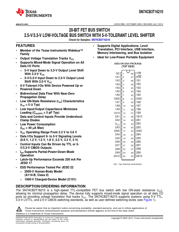
DGG OR DGV PACKAGE (TOP VIEW)
NC 1 1A1 2 1A2 3 1A3 4 1A4 5 1A5 6 1A6 7 GND 8 1A...