SN74CBT16245C 16ĆBIT FET BUS SWITCH 5ĆV BUS SWITCH WITH -2ĆV UNDERSHOOT PROTECTION
SCDS139 − OCTOBER 2003
D Member of t...
SN74CBT16245C 16ĆBIT FET BUS SWITCH 5ĆV BUS SWITCH WITH -2ĆV UNDERSHOOT PROTECTION
SCDS139 − OCTOBER 2003
D Member of the Texas Instruments
Widebus Family
D Undershoot Protection for Off-Isolation on
A and B Ports Up to −2 V
D Bidirectional Data Flow, With Near-Zero
Propagation Delay
D Low ON-State Resistance (ron)
Characteristics (ron = 3 Ω Typical)
D Low Input/Output Capacitance Minimizes
Loading and Signal Distortion (Cio(OFF) = 5.5 pF Typical)
D Data and Control Inputs Provide
Undershoot Clamp Diodes
D Low Power Consumption
(ICC = 3 µA Max)
D VCC Operating Range From 4 V to 5.5 V D Data I/Os Support 0 to 5-V Signaling Levels
(0.8-V, 1.2-V, 1.5-V, 1.8-V, 2.5-V, 3.3-V, 5-V)
D Control Inputs Can be Driven by TTL or
5-V/3.3-V
CMOS Outputs
D Ioff Supports Partial-Power-Down Mode
Operation
D Latch-Up Performance Exceeds 100 mA Per
JESD 78, Class II
D ESD Performance Tested Per JESD 22
− 2000-V Human-Body Model (A114-B, Class II)
− 1000-V Charged-Device Model (C101)
D Supports Both Digital and Analog
Applications: PCI Interface, Memory Interleaving, Bus Isolation, Low-Distortion Signal Gating
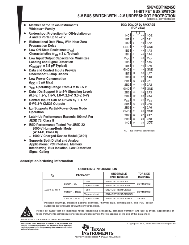
DGG, DGV, OR DL PACKAGE (TOP VIEW)
NC 1 1B1 2 1B2 3 GND 4 1B3 5 1B4 6 VCC 7 1B5 8 1B6 9 GND 10 1B7 11 1B8 12 2B1 13 2B2 14 GND 15 2B3 16 2B4 17 VCC 18 2B5 19 2B6 20 GND 21 2B7 22 2B8 23 NC 24
48 1OE 47 1A1 46 1A2 45 GND 44 1A3 43 1A4 42 VCC 41 1A5 40 1A6 39 GND 38 1A7 37 1A8 36 2A1 35 2A2 34 GND 33 2A3 32 2A4 31 VCC 30 2A5 29 2A6 28 GND 27 2A7 26 2A8 25 2OE
NC − No internal connection...