SN74CBT3245C 8ĆBIT FET BUS SWITCH 5ĆV BUS SWITCH WITH ć2ĆV UNDERSHOOT PROTECTION
SCDS131A − SEPTEMBER 2003 − REVISED OCT...
SN74CBT3245C 8ĆBIT FET BUS SWITCH 5ĆV BUS SWITCH WITH ć2ĆV UNDERSHOOT PROTECTION
SCDS131A − SEPTEMBER 2003 − REVISED OCTOBER 2003
D Undershoot Protection for Off-Isolation on
A and B Ports Up To −2 V
D Bidirectional Data Flow, With Near-Zero
Propagation Delay
D Low ON-State Resistance (ron)
Characteristics (ron = 3 Ω Typical)
D Low Input/Output Capacitance Minimizes
Loading and Signal Distortion
(Cio(OFF) = 5.5 pF Typical)
D Data and Control Inputs Provide
Undershoot Clamp Diodes
D Low Power Consumption
(ICC = 3 µA Max)
D VCC Operating Range From 4 V to 5.5 V D Data I/Os Support 0 to 5-V Signaling Levels
(0.8-V, 1.2-V, 1.5-V, 1.8-V, 2.5-V, 3.3-V, 5-V)
D Control Inputs Can Be Driven by TTL or
5-V/3.3-V
CMOS Outputs
D Ioff Supports Partial-Power-Down Mode
Operation
D Latch-Up Performance Exceeds 100 mA Per
JESD 78, Class II
D ESD Performance Tested Per JESD 22
− 2000-V Human-Body Model (A114-B, Class II)
− 1000-V Charged-Device Model (C101)
D Supports Both Digital and Analog
Applications: USB Interface, Memory Interleaving, Bus Isolation, Low-Distortion Signal Gating
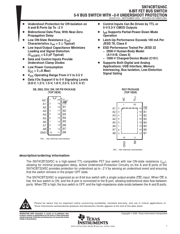
DB, DBQ, DGV, DW, OR PW PACKAGE (TOP VIEW)
RGY PACKAGE (TOP VIEW)
VCC
NC
NC 1 A1 2 A2 3 A3 4 A4 5 A5 6 A6 7 A7 8 A8 9 GND 10
20 VCC 19 OE 18 B1 17 B2 16 B3 15 B4 14 B5 13 B6 12 B7 11 B8
NC − No internal connection
1 A1 2 A2 3 A3 4 A4 5 A5 6 A6 7 A7 8 A8 9
10
20 19 OE 18 B1 17 B2 16 B3 15 B4 14 B5 13 B6 12 B7
11
B8
GND
NC − No internal connection
description/ordering information
The SN74CBT3245C is a h...