10-BIT FET BUS SWITCH
SN74CBT3861 10-BIT FET BUS SWITCH
D 5-Ω Switch Connection Between Two Ports D TTL-Compatible Input Levels D Latch-Up Pe...
Description
SN74CBT3861 10-BIT FET BUS SWITCH
D 5-Ω Switch Connection Between Two Ports D TTL-Compatible Input Levels D Latch-Up Performance Exceeds 250 mA Per
JESD 17
description
The SN74CBT3861 provides ten bits of high-speed TTL-compatible bus switching. The low on-state resistance of the switch allows connections to be made with minimal propagation delay.
The device is organized as one 10-bit switch with a single output-enable (OE) input. When OE is low, the switch is on, and port A is connected to port B. When OE is high, the switch is open, and the high-impedance state exists between the two ports.
SCDS061D – APRIL 1998 – REVISED OCTOBER 2000
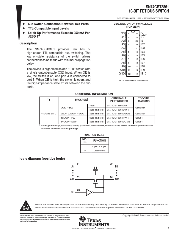
DBQ, DGV, DW, OR PW PACKAGE (TOP VIEW)
NC 1 A1 2 A2 3 A3 4 A4 5 A5 6 A6 7 A7 8 A8 9 A9 10 A10 11 GND 12
24 VCC 23 OE 22 B1 21 B2 20 B3 19 B4 18 B5 17 B6 16 B7 15 B8 14 B9 13 B10
NC – No internal connection
ORDERING INFORMATION
TA
PACKAGE†
ORDERABLE PART NUMBER
TOP-SIDE MARKING
SOIC – DW
Tube
SN74CBT3861DW
Tape and reel SN74CBT3861DWR
CBT3861
–40°C to 85°C SSOP (QSOP) – DBQ Tape and reel SN74CBT3861DBQR CBT3861
TSSOP – PW
Tape and reel SN74CBT3861PWR
CU861
TVSOP – DGV
Tape and reel SN74CBT3861DGVR CU861
† Package drawings, standard packing quantities, thermal data, symbolization, and PCB design guidelines are available at www.ti.com/sc/package.
FUNCTION TABLE
INPUT OE
FUNCTION
L A port = B port
H
Disconnect
logic diagram (positive logic)
2 A1
22 B1
11 A10
13 B10
23 OE
Please be aware that an important notice c...
Similar Datasheet