QUADRUPLE BUS BUFFER GATE
D 3-State Outputs Drive Bus Lines or Buffer
Memory Address Registers
description/ordering information The SN74F125 featu...
Description
D 3-State Outputs Drive Bus Lines or Buffer
Memory Address Registers
description/ordering information The SN74F125 features independent line drivers with 3-state outputs. Each output is disabled when the associated output-enable (OE) input is high.
SN74F125 QUADRUPLE BUS BUFFER GATE
WITH 3-STATE OUTPUTS
SDFS016B – JANUARY 1989 – REVISED JULY 2002
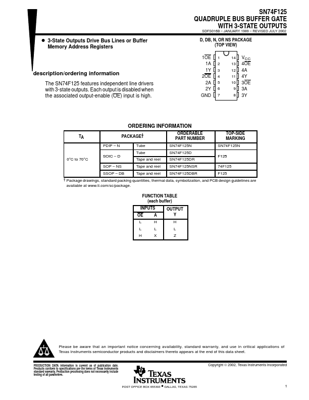
D, DB, N, OR NS PACKAGE (TOP VIEW)
1OE 1 1A 2 1Y 3
2OE 4 2A 5 2Y 6
GND 7
14 VCC 13 4OE 12 4A 11 4Y 10 3OE 9 3A 8 3Y
ORDERING INFORMATION
TA
PACKAGE†
ORDERABLE PART NUMBER
TOP-SIDE MARKING
PDIP – N
Tube
SN74F125N
SN74F125N
0°C to 70°C
SOIC – D
Tube Tape and reel
SN74F125D SN74F125DR
F125
SOP – NS
Tape and reel SN74F125NSR
74F125
SSOP – DB
Tape and reel SN74F125DBR
F125
† Package drawings, standard packing quantities, thermal data, symbolization, and PCB design guidelines are available at www.ti.com/sc/package.
FUNCTION TABLE (each buffer)
INPUTS
OE
A
OUTPUT Y
L
H
H
L
L
L
H
X
Z
Please be aware that an important notice concerning availability, standard warranty, and use in critical applications of Texas Instruments semiconductor products and disclaimers thereto appears at the end of this data sheet.
PRODUCTION DATA information is current as of publication date. Products conform to specifications per the terms of Texas Instruments standard warranty. Production processing does not necessarily include testing of all parameters.
POST OFFICE BOX 655303 DALLAS, TEXAS 75265
Copyright 2002, Texas Ins...
Similar Datasheet