• Contains Six Flip-Flops With Single-Rail
Outputs
• Buffered Clock and Direct Clear Inputs • Applications Include:
Buff...
Contains Six Flip-Flops With Single-Rail
Outputs
Buffered Clock and Direct Clear Inputs Applications Include:
Buffer/Storage Registers
Shift Registers
Pattern Generators
Fully Buffered Outputs for Maximum
Isolation From External Disturbances
Package Options Include Plastic
Small-Outline Packages and Standard
Plastic 300-mil DIPs
SN74F174A HEX D-TYPE FLIP-FLOP
WITH CLEAR
SDFS029B – D2932, MARCH 1987 – REVISED OCTOBER 1993
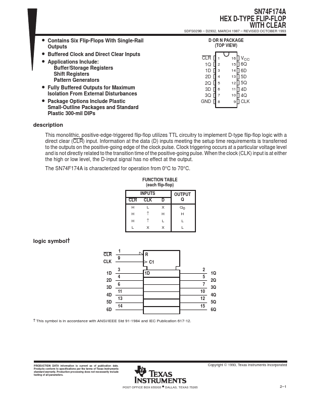
D OR N PACKAGE (TOP VIEW)
CLR 1 1Q 2 1D 3 2D 4 2Q 5 3D 6 3Q 7
GND 8
16 VCC 15 6Q 14 6D 13 5D 12 5Q 11 4D 10 4Q 9 CLK
description
This monolithic, positive-edge-triggered flip-flop utilizes TTL circuitry to implement D-type flip-flop logic with a direct clear (CLR) input. Information at the data (D) inputs meeting the setup time requirements is transferred to the outputs on the positive-going edge of the clock pulse. Clock triggering occurs at a particular
voltage level and is not directly related to the transition time of the positive-going pulse. When the clock (CLK) input is at either the high or low level, the D-input signal has no effect at the output.
The SN74F174A is characterized for operation from 0°C to 70°C.
FUNCTION TABLE (each flip-flop)
INPUTS
CLR CLK D
H
L
X
H
↑
H
H
↑
L
L
X
X
OUTPUT Q
Q0 H L L
logic symbol†
1 CLR
9 CLK
3 1D
4 2D
6 3D
11 4D
13 5D
14 6D
R C1
1D
† This symbol is in accordance with ANSI/IEEE Std 91-1984 and IEC Publication 617-12.
2 1Q
5 2Q
7 3Q
10 4Q
12 5Q
15 6Q
PRODUCTION DATA information is cur...