8-BIT UNIVERSAL SHIFT/STORAGE REGISTERS
ą
The SN54F299 is obsolete and no longer supplied.
SN54F299, SN74F299 8ĆBIT UNIVERSAL SHIFT/STORAGE REGISTERS
WITH 3ĆST...
Description
ą
The SN54F299 is obsolete and no longer supplied.
SN54F299, SN74F299 8ĆBIT UNIVERSAL SHIFT/STORAGE REGISTERS
WITH 3ĆSTATE OUTPUTSą
SDFS071B − MARCH 1987 − REVISED APRIL 2004
D Four Modes of Operation:
− Hold (Store) − Shift Right − Shift Left − Load Data
D Operates With Outputs Enabled or at High
Impedance
D 3-State Outputs Drive Bus Lines Directly D Can Be Cascaded for N-Bit Word Lengths D Direct Overriding Clear D Applications:
− Stacked or Pushdown Registers − Buffer Storage − Accumulator Registers
description/ordering information
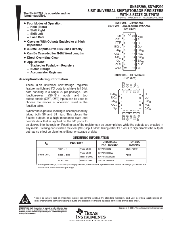
SN54F299 . . . J PACKAGE SN74F299 . . . DW, N, OR NS PACKAGE
(TOP VIEW)
S0 1
OE1 2
OE2 3
G/QG 4 E/QE 5 C/QC 6 A/QA 7
QA′ 8 CLR 9
GND 10
20 VCC 19 S1
18 SL
17 QH′ 16 H/QH 15 F/QF 14 D/QD 13 B/QB 12 CLK
11 SR
SN54F299 . . . FK PACKAGE (TOP VIEW)
OE2 OE1 S0 VCC S1
These 8-bit universal shift /storage registers
feature multiplexed I/O ports to achieve full 8-bit
data handling in a single 20-pin package. Two function-select (S0, S1) inputs and two output-enable (OE1, OE2) inputs can be used to choose the modes of operation listed in the function table.
Synchronous parallel loading is accomplished by
G/QG E/QE C/QC A/QA
QA′
3 2 1 20 19
4
18
5
17
6
16
7
15
8
14
9 10 11 12 13
SL
QH′ H/QH F/QF D/QD
taking both S0 and S1 high. This places the
CLR GND
SR CLK B/QB
3-state outputs in a high-impedance state and
permits data that is applied on the I/O ports to
be clocked into the register. Reading out of the register can be accompl...
Similar Datasheet