OCTAL BUFFERS/DRIVERS
• 3-State Outputs Drive Bus Lines or Buffer
Memory Address Registers
• Data Flow-Through Pinout (All Inputs on
Opposite ...
Description
3-State Outputs Drive Bus Lines or Buffer
Memory Address Registers
Data Flow-Through Pinout (All Inputs on
Opposite Side From Outputs)
Package Options Include Plastic
Small-Outline Packages, Ceramic Chip Carriers, and Plastic and Ceramic DIPs
description
The ′F541 octal buffer/line driver is ideal for driving bus lines or buffering memory address registers. The device features inputs and outputs on opposite sides of the package to facilitate printed-circuit-board layout.
The 3-state control gate is a 2-input AND gate with active-low inputs so that if either output enable (OE1 or OE2) input is high, all eight outputs are in the high-impedance state.
The SN54F541 is characterized for operation over the full military temperature range of – 55°C to 125°C. The SN74F251 is characterized for operation from 0°C to 70°C.
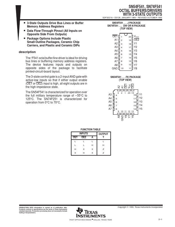
SN54F541, SN74F541 OCTAL BUFFERS/DRIVERS
WITH 3-STATE OUTPUTS
SDFS021A – D3126, JANUARY 1989 – REVISED OCTOBER 1993
SN54F541 . . . J PACKAGE SN74F541 . . . DW OR N PACKAGE
(TOP VIEW)
OE1 1 A1 2 A2 3 A3 4 A4 5 A5 6 A6 7 A7 8 A8 9
GND 10
20 VCC 19 OE2 18 Y1 17 Y2 16 Y3 15 Y4 14 Y5 13 Y6 12 Y7 11 Y8
SN54F541 . . . FK PACKAGE (TOP VIEW)
A2 A1 OE1 VC C OE2
A3
3 2 1 20 19
4
18
Y1
A4 5
17 Y2
A5 6
16 Y3
A6 7
15 Y4
A7 8
14 Y5
9 10 11 12 13
A8 GND
Y8 Y7 Y6
FUNCTION TABLE
INPUTS OE1 OE2 A
OUTPUT Y
L
L
L
L
L
L
H
H
H
X
X
Z
X
H
X
Z
PRODUCTION DATA information is current as of publication date. Products conform to specifications per the ...
Similar Datasheet